
Date:2026-03-17 Categories:Application Cases Hits:686 From:Guangdong Youfeng Microelectronics Co., Ltd
This article is sourced from Charging Head Network. If there is any infringement, please contact the author for timely removal
Preface
Beishida has launched a 33W fast charging charger K26, which features a white straight body design, national standard fixed pins, and a simple appearance. This charger has a 2A1C fast charging interface, a USB-C interface that supports 30W PD fast charging, and a USB-A interface that supports 27W fast charging. All three interfaces support fast charging.
When using this charger with both USB-C and USB-A ports, the USB-C port can still maintain fast charging output, providing a better user experience. Below is the disassembly of this charger from the charging head network, let's take a look at the internal design and materials.
Appearance of Beishida 33W charger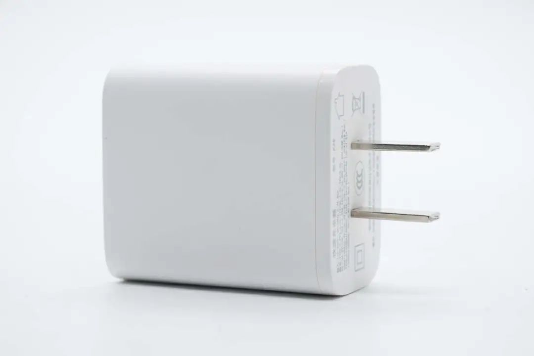
The charger adopts a straight board design, with a white shell and a classic main body frosted surface with bright edge accents.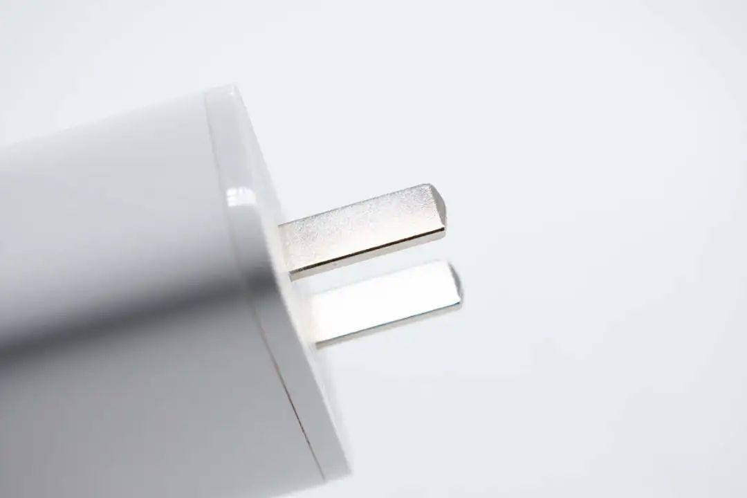
The charger is equipped with fixed national standard pins.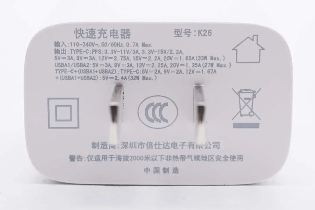
The input shell is printed with charger parameters
Model: K26
Input: 110-240V~50/60Hz 0.7A Max
output:
Type-C:5V3A、9V3A、12V2.75A、15V2.2A、20V1.65A(33W Max)
PPS:3.3-11V3A、3.3-15V2.2A
USB-A1/A2:5V3A、9V3A、12V2.25A、20V1.35A(27W Max)
Type-C+(USB-A1+USB-A2):20W+12W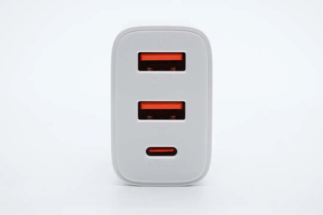
The charger output terminal is equipped with three USB ports, 2A1C, and the rubber cores are all in a prominent orange color scheme.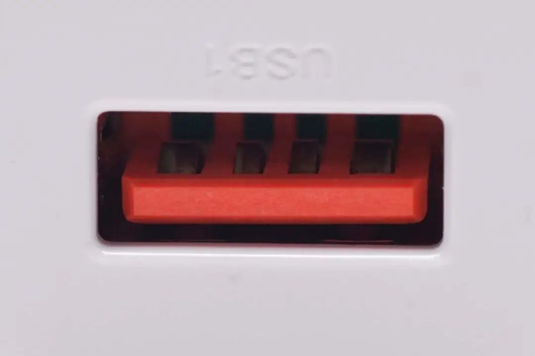
Close up of USB-A port rubber core, with widened positive and negative electrodes designed for excessive current.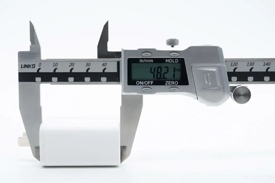
The measured height of the charger body is 48.21mm.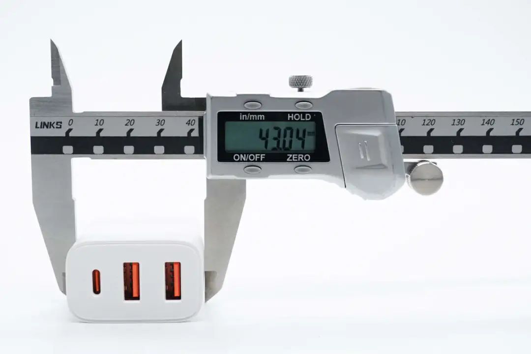
The width is 43.04mm.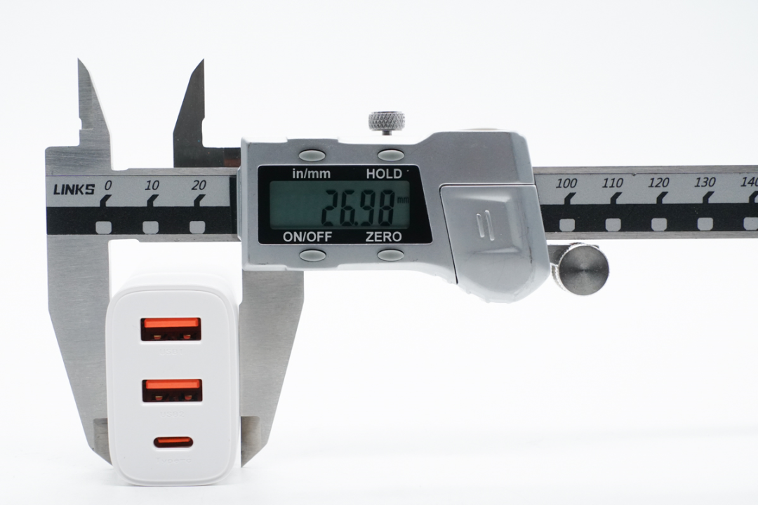
The thickness is 26.98mm.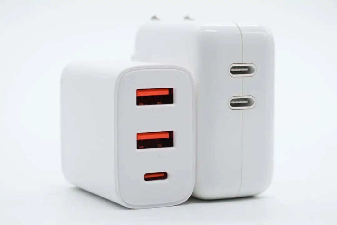
Compared to the Apple 35W charger, the Beishida model is slightly smaller in size.
The size of the charger in the hand is intuitively felt.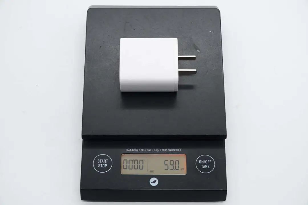
Additionally, the net weight of the charger was measured to be approximately 59g.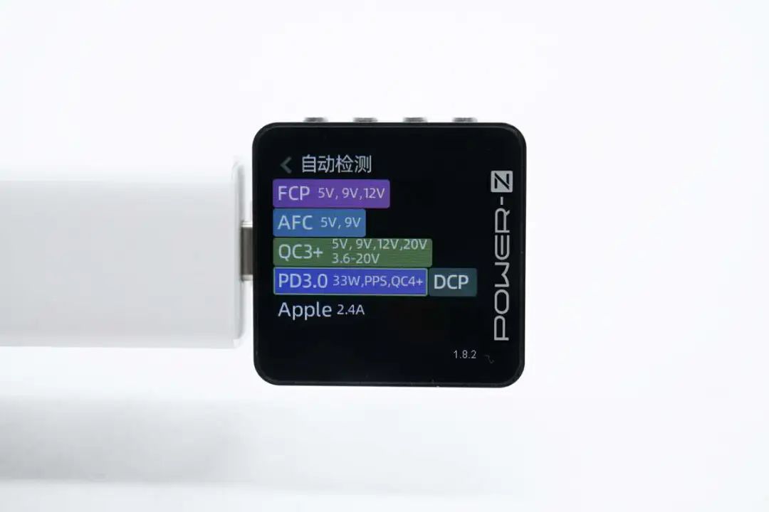
Using ChargerLAB POWER-Z KM003C, it was measured that the USB-C port supports FCP, AFC, QC3+/4+, PD3.0, PPS, DCP, and Apple 2.4A charging protocols.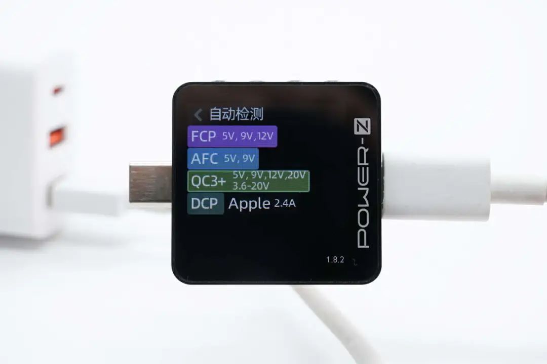
The PDO message shows that the USB-C port also has five fixed voltage levels: 5V3A, 9V3A, 12V2.75A, 15V2.2A, and 20V1.65A, as well as two PPS voltage levels: 3.3-11V3A and 3.3-15V2.2A.
The USB-A1 port has been tested to support FCP, AFC, QC3+, DCP, and Apple 2.4A charging protocols.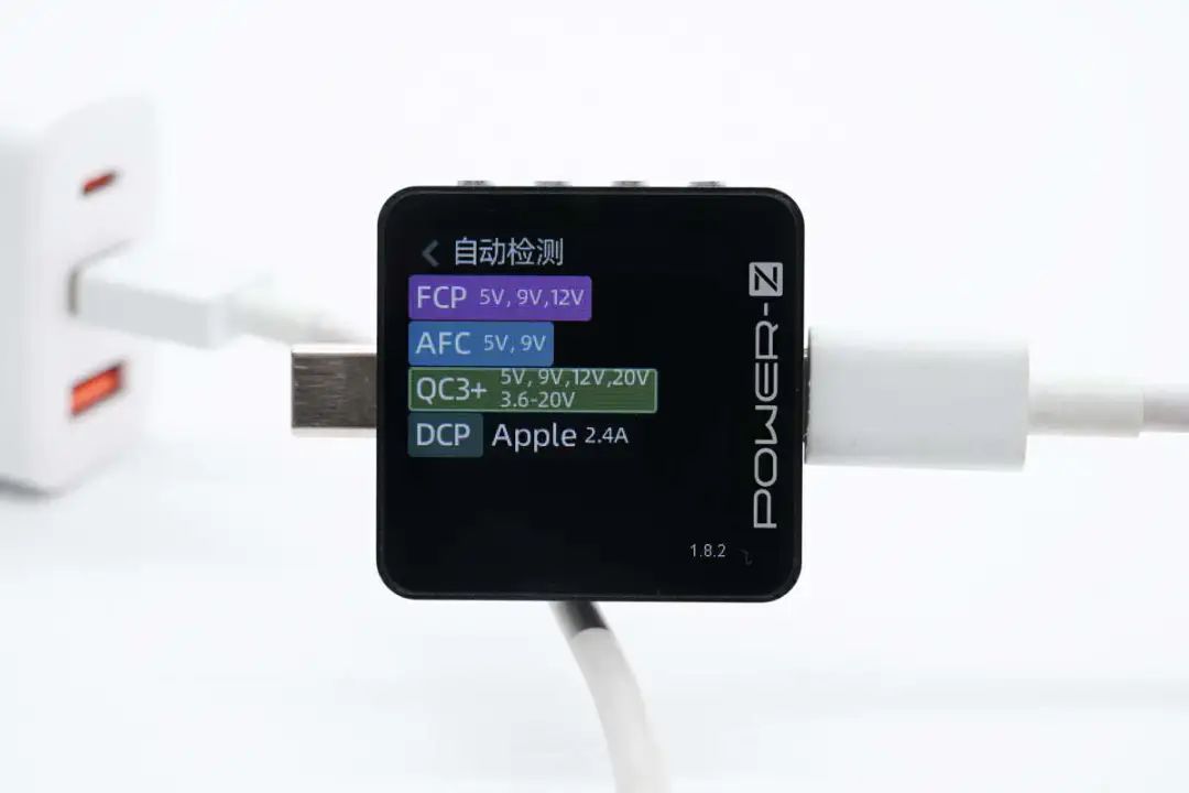
The compatibility protocol of USB-A2 port and USB-A1 port were tested to be the same.
Dismantling of Beishida 33W charger
After reading the unboxing and testing of the Beishida 33W charger, let's disassemble it and take a look at the internal design and materials.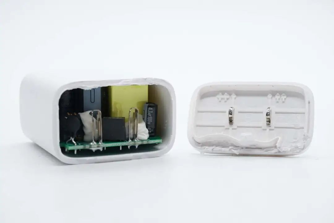
Firstly, pry open the ultrasonic welded charger housing along the seam, and connect the pins to the power supply through a clip.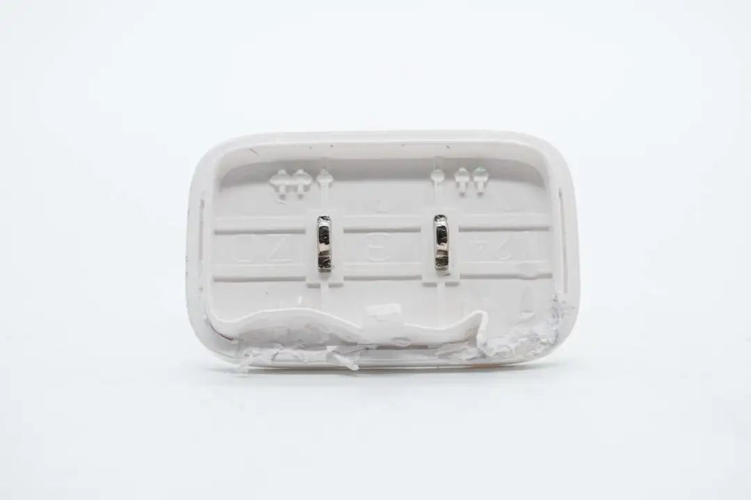
The protruding pins are connected to the charger PCBA module clip.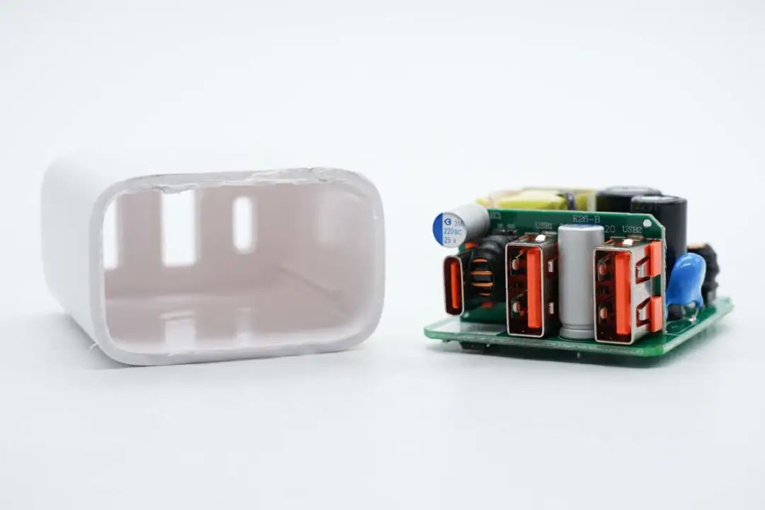
Extract the PCBA module from the interior of the housing and create a positioning slot inside the housing to secure the PCBA module.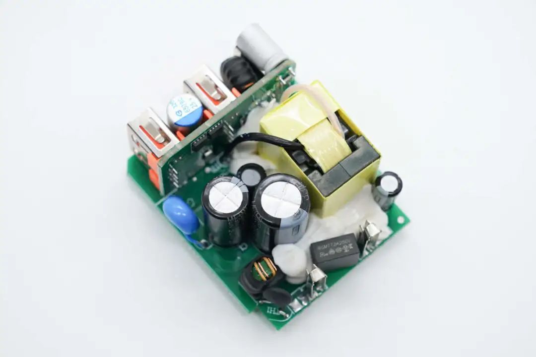
The PCBA module is composed of two PCBs welded together, and the transformer is reinforced with glue.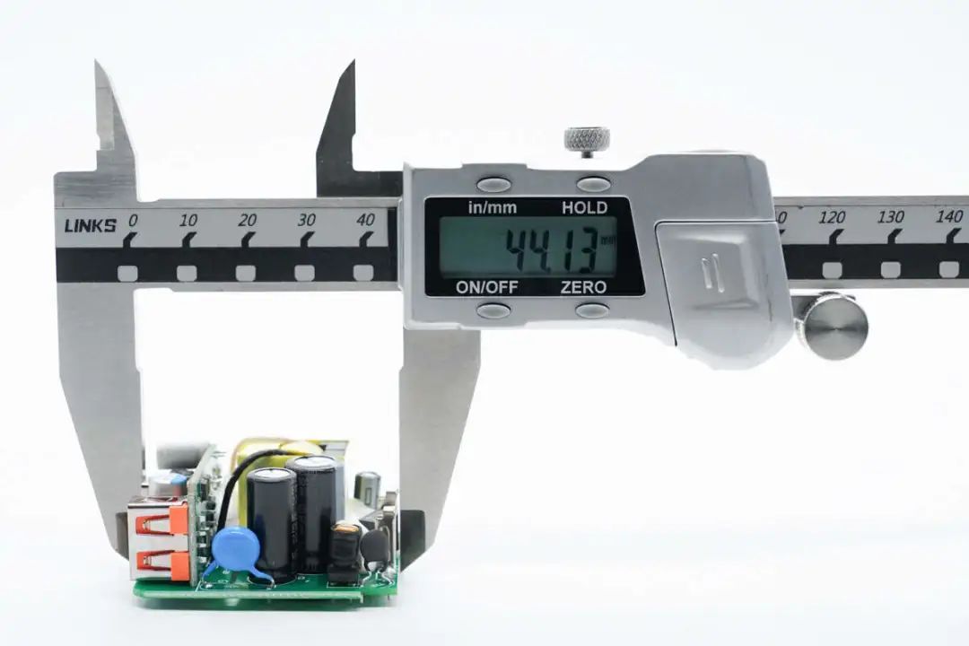
The length of the PCBA module measured using a vernier caliper is approximately 44.1mm.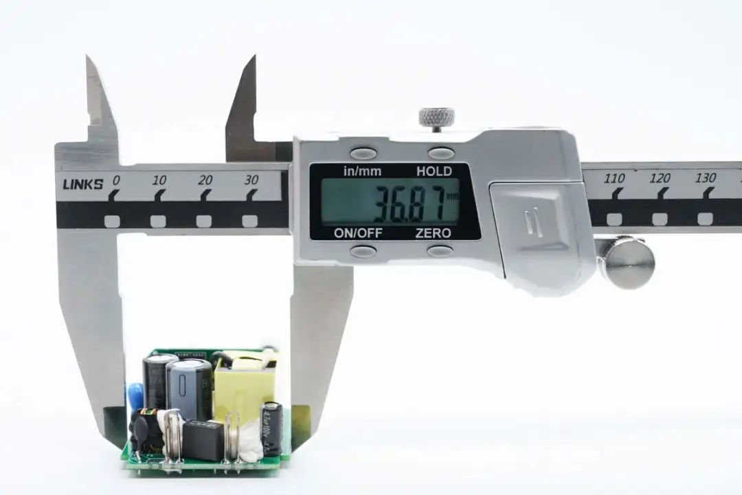
The width of the PCBA module is approximately 36.9mm.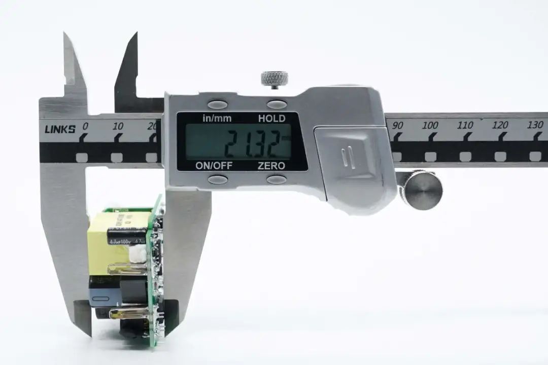
The thickness of the PCBA module is approximately 21.3mm.
Front view of PCBA module, with fuse soldered on the left input end, NTC surge suppression resistor and common mode inductor soldered on the top, high-voltage filter capacitor and differential mode inductor soldered on the right, and transformer soldered on the bottom. Weld the output voltage reducing plate and filtering capacitor on the right side.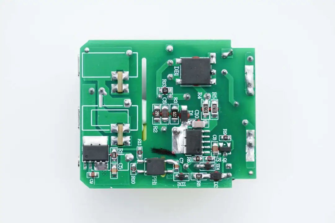
The back of the PCBA module is soldered with rectifier bridge, primary power chip, feedback optocoupler, synchronous rectifier chip, and the circuit is very simple. The PCB is insulated with slots between the primary stages.
Through observation of the PCBA module, it was found that the 33W charger from Beishida adopts the Biyi Micro flyback switch power supply scheme, using KP22315A with KP40512. The output voltage is fed back by the protocol chip through optocouplers, and the circuit is very simple. The protocol chip adopts Cloud Silicon Semiconductor XPD913, with built-in buck converter and 2A1C interface configuration. When USB-C fast charging output, the USB-A interface has 5V output. Let's start learning about the information of each component from the input end.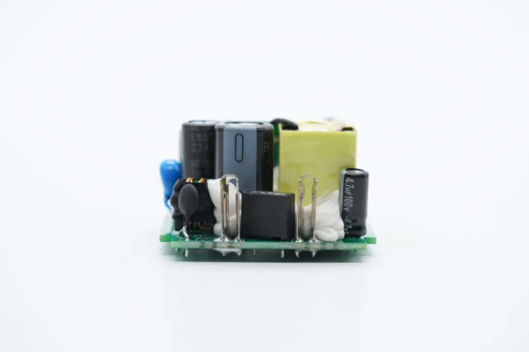
Weld a fuse between the AC input terminal clips of the charger, and weld NTC surge suppression resistors, common mode inductors, and filtering capacitors that supply power to the main control chip on both sides.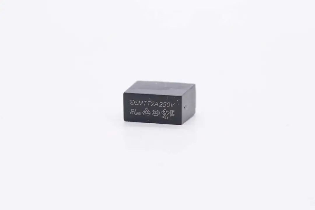
The input fuse specification is 2A 250V.
NTC surge suppression resistor silk screen 5D-5.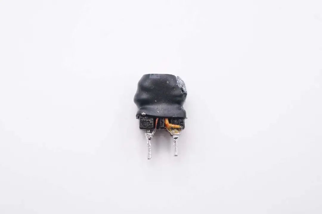
The common mode inductor is made of enameled wire and insulated wire winding, insulated with a heat shrink tubing jacket, and welded with an insulated bracket at the bottom.
The rectifier bridge is from Yufengwei, model FMB30M, with a specification of 3A 1000V. Adopting UMSB packaging, YFW Youfeng Micro brand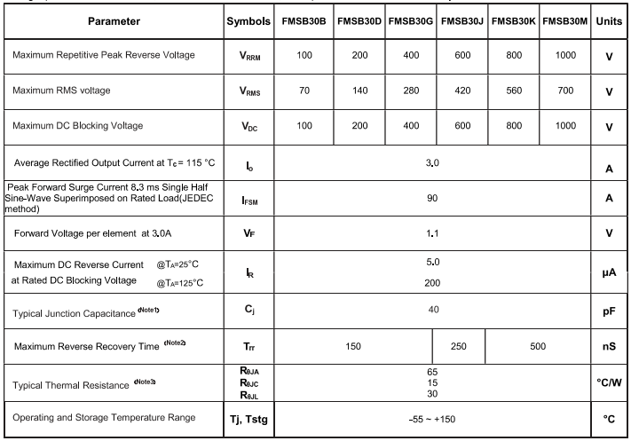
Yufeng Microelectronics "is a high-tech enterprise specializing in the research and development, production, and sales of semiconductor discrete devices. The company mainly produces and sells: ordinary rectifier diodes, fast recovery diodes, high-efficiency diodes, ultrafast recovery diodes, Schottky diodes, low voltage drop Schottky diodes, silicon carbide diodes, rectifier bridge stacks, fast recovery rectifier bridge stacks, Schottky bridge stacks, TVS transient suppression diodes, ESD electrostatic protection components, voltage regulators, transistors, thyristors, MOSFETs, and so on. For more details, please visit our official website www.yfwdiode.com.
Previous: USB interface 2.0, ESD protection solution from Youfeng Microelectronics
