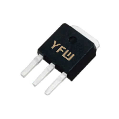
A BJT consists of three semiconductor layers: the emitter, base, and collector. These layers form two PN junctions: the emitter-base junction and the collector-base junction. There are two primary types of BJTs: NPN (Negative-Positive-Negative) and PNP (Positive-Negative-Positive), differing in the arrangement of doped semiconductor materials .
NPN Transistor: Comprises an N-type emitter, P-type base, and N-type collector. Electrons are the majority charge carriers.
PNP Transistor: Features a P-type emitter, N-type base, and P-type collector. Holes dominate the current flow.
Both types share the same fundamental operating principle but require opposite biasing conditions. For example, an NPN transistor needs forward bias on the emitter-base junction and reverse bias on the collector-base junction to operate in the active region .
The operation of a BJT is governed by the flow of charge carriers across its junctions. Let’s take an NPN transistor as an example:
Emitter-Base Junction Forward Bias: When a small forward voltage (e.g., 0.7V for silicon) is applied between the base and emitter, the depletion region narrows, allowing majority carriers (electrons in NPN) to flow from the emitter to the base .
Base Region: The base is lightly doped and thin, so only a small fraction of electrons recombine with holes, creating a small base current (I_B). The remaining electrons diffuse into the collector region.
Collector-Base Junction Reverse Bias: The reverse-biased collector-base junction attracts the diffused electrons from the base, resulting in a large collector current (I_C). The relationship between I_C and I_B is defined by the current gain (β), where I_C = β × I_B .
This mechanism allows a small base current to control a much larger collector current, making the BJT a current-controlled device. The power delivered to the load (via I_C) is significantly higher than the input power (I_B), enabling signal amplification .
BJTs operate in three distinct regions, each with specific applications:
Cutoff Region: Both junctions are reverse-biased. No current flows between the collector and emitter (I_C ≈ 0). This region is used for switching applications to turn circuits off .
Active Region: The emitter-base junction is forward-biased, and the collector-base junction is reverse-biased. Here, I_C is proportional to I_B, making this region ideal for signal amplification. YFW’s small-signal transistors, such as the MMBT2222A and BFS20, are optimized for linear amplification in audio and RF circuits .
Saturation Region: Both junctions are forward-biased. The collector current reaches its maximum value (I_C(sat)), and the voltage drop across the collector-emitter (V_CE) is minimal. This region is used in switching applications to turn circuits fully on .
To ensure optimal performance, designers must consider critical parameters:
Current Gain (β): The ratio of I_C to I_B. YFW’s transistors offer a wide range of β values (e.g., 60–150 for the 2SA1013-Y), catering to diverse amplification needs .
Voltage Ratings: Maximum allowable voltages across junctions (e.g., V_CEO = 160V for the 2SA1013-Y) .
Power Dissipation: The ability to handle heat generated during operation. YFW’s power transistors, such as those in the TO-220 package, are designed for high-power applications like motor control and power supplies .
Frequency Response: High-frequency transistors (e.g., YFW’s BFS20) excel in RF amplifiers and oscillators due to their fast switching speeds .
BJTs are integral to countless electronic systems:
Amplifiers: Used in audio systems, operational amplifiers, and RF transmitters to boost weak signals. YFW’s low-noise transistors ensure high-fidelity amplification .
Switches: Control power flow in circuits, such as in automotive ignition systems and relay drivers. YFW’s transistors in SOT-23 and TO-252 packages offer compact, reliable switching solutions .
Voltage Regulators: Maintain stable output voltages in power supplies by adjusting current flow .
Digital Logic: Form the basis of logic gates in microprocessors and memory devices .
As a leading semiconductor manufacturer, YFW specializes in producing high-quality BJTs tailored for reliability and efficiency. Our product portfolio includes:
Small-Signal Transistors: Ideal for low-power applications like signal conditioning and amplification (e.g., BC858AW and BFS520W) .
Power Transistors: Designed for high-current and high-voltage scenarios, such as motor drives and power inverters.
High-Frequency Transistors: Optimized for RF and microwave applications, ensuring superior performance in communication systems.
Third-Generation Semiconductor Devices: Leveraging advanced materials like SiC for enhanced thermal stability and efficiency .
All YFW transistors undergo rigorous testing to meet international standards (e.g., RoHS), ensuring consistent performance across diverse operating conditions . Our commitment to innovation and customer-centric design makes us a trusted partner for industries ranging from consumer electronics to renewable energy .
The working principle of a BJT hinges on its ability to control current flow through the manipulation of charge carriers in its semiconductor layers. By understanding the interplay between biasing conditions, current gain, and operating regions, engineers can harness BJTs for amplification, switching, and signal processing. YFW’s comprehensive range of transistors, backed by cutting-edge technology and stringent quality control, empowers designers to create robust and efficient electronic systems. Whether in audio amplifiers, automotive electronics, or industrial automation, YFW’s transistors deliver the performance and reliability required for modern applications.
