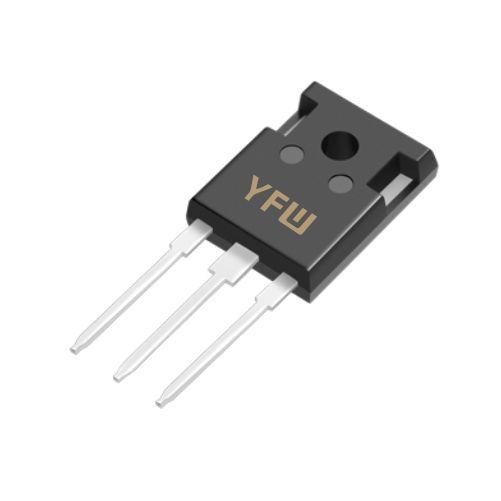
SiC MOSFETs outperform silicon-based devices in efficiency and power density, but their maximum current ratings are often insufficient for applications requiring hundreds or thousands of amperes. For example, a single 1200V
SiC MOSFET might handle 100A, but a 500A system demands five such devices in parallel. By distributing the load across multiple transistors, paralleling increases the total current capacity while reducing individual device stress. This approach also enhances redundancy, as failing devices can be bypassed without system shutdown.
However,
SiC MOSFETs are highly sensitive to parameter variations and parasitic effects. Unlike silicon devices,
SiC MOSFETs exhibit a positive temperature coefficient in Rds(on), which means hotter devices conduct less current—a self-balancing mechanism. Yet, dynamic current sharing during switching remains problematic due to parasitic inductance and gate charge (Qg) mismatches. Without proper design, these factors can lead to catastrophic failures.
Device-to-device variations in threshold voltage (Vth), Rds (on), and Qg cause unequal current distribution. A 10% Rds (on) mismatch can lead to a 20% current imbalance, increasing power loss and thermal stress in the weaker device . Vth differences affect turn-on/off timing, exacerbating dynamic Uneven flow.
Parasitic inductance in the power loop and gate drive circuitry creates voltage spikes during switching. Asymmetric layouts cause unequal inductance, leading to current sharing issues. Even a 5nH difference in source inductance can result in a 20% current deviation during turn-off .
Uneven current distribution causes localized hotspots. SiC MOSFETs operate at higher temperatures (up to 175°C), and thermal runaway can occur if heat dissipation is inadequate. The positive temperature coefficient of Rds(on) helps mitigate this but requires precise thermal design .
SiC MOSFETs demand fast, synchronized gate signals to minimize switching losses. Asymmetric drive paths or inadequate gate resistors (Rg) introduce delays, worsening dynamic Uneven flow.
Parameter Screening: Select devices with tightly matched Vth (±0.1V) and Rds(on) (±5%). YFW’s SiC MOSFETs undergo rigorous testing to ensure batch-to-batch consistency, reducing pre-screening efforts .
Package Symmetry: Choose packages with low parasitic inductance, such as YFW’s TOLL or D2PAK variants. These designs minimize inductive mismatch and improve thermal dissipation .
Symmetric Power Traces: Route drain and source connections symmetrically to balance inductance. Use wide, short traces to reduce resistance and inductance.
Gate Drive Isolation: Separate power and signal traces to avoid crosstalk. Place gate drivers close to the MOSFETs to minimize parasitic inductance in the gate loop .
Decoupling Capacitors: Add ceramic capacitors near each MOSFET to stabilize the gate voltage and suppress high-frequency noise.
Passive Techniques:
Source Inductors: Add small inductors (1–5nH) in series with each source to equalize dynamic current sharing.
Resistive Ballasting: Insert a 0.1–0.5Ω resistor in each drain path to balance static current. While this increases conduction loss, it ensures stability in high-power applications .
Active Techniques:
Dynamic Gate Control: Use active gate drivers (AGD) to adjust gate resistance dynamically, compensating for parameter variations. YFW’s AGD solutions can reduce current imbalance by up to 80% .
Current Sensing Feedback: Implement closed-loop control with current sensors to monitor and adjust device currents in real time.
Heat Sink Optimization: Use high-conductivity materials (e.g., copper) and finned heat sinks to maximize heat dissipation. YFW’s SiC MOSFETs feature low thermal resistance (RθJC < 2°C/W), enabling efficient heat transfer .
Thermal Interface Materials: Apply thermal paste or pads with low thermal resistance to ensure good contact between the device and heat sink.
Temperature Monitoring: Integrate thermal sensors to detect hotspots and trigger cooling mechanisms or derating if needed.
Isolated Gate Drivers: Use isolated drivers with high common-mode transient immunity (CMTI) to protect against high dV/dt noise. YFW’s gate drivers support ±20V operation and fast switching (tr < 5ns) .
Gate Resistance Configuration: Combine a common gate resistor (Rg_common) for stability and individual resistors (Rg_individual) to control switching speed. This hybrid approach balances oscillation suppression and current sharing .
Miller Clamping: Add Miller clamp circuits to prevent parasitic turn-on during high dV/dt events, especially in half-bridge configurations .
YFW recently developed a 300kW three-phase inverter using eight paralleled YFW1200V SiC MOSFETs. The design incorporated the following innovations:
Symmetric Layout: A four-layer PCB with mirrored power traces reduced parasitic inductance to <10nH.
Active Gate Control: YFW’s AGD-200 driver adjusted gate resistance dynamically, achieving a current imbalance <5% under full load.
Thermal Management: A liquid-cooled cold plate with integrated temperature sensors maintained junction temperatures below 150°C, ensuring reliability over 10,000 hours .
Paralleling SiC MOSFETs is a viable strategy to achieve higher power levels, but it requires careful attention to device matching, layout symmetry, and thermal management. By leveraging YFW’s advanced SiC MOSFETs and innovative drive solutions, engineers can design robust, high-efficiency systems for next-generation applications. Whether in EV fast chargers, solar inverters, or industrial motor drives, YFW’s technology ensures optimal performance and reliability. For customized solutions, contact YFW’s engineering team to explore how our SiC MOSFETs can meet your power requirements.
YFW: Empowering High-Power Electronics with Silicon Carbide Innovation
