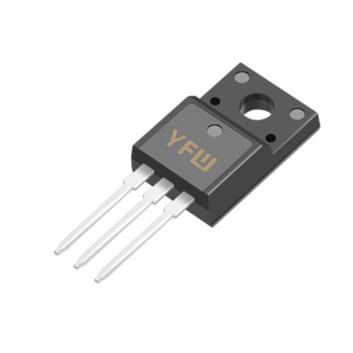
A UJT consists of a lightly doped N-type silicon bar with two ohmic contacts at its ends, designated as Base 1 (B1) and Base 2 (B2) . A heavily doped P-type emitter (E) is alloyed onto one side of the silicon bar, forming a single PN junction—hence the term "unijunction" . The emitter is strategically positioned closer to B2 than B1 to create an asymmetric structure, optimizing its electrical performance for practical applications .
The silicon bar between B1 and B2 exhibits high resistivity, typically ranging from 4 to 10 kΩ when the emitter is open . This resistivity arises from the low doping concentration of the N-type material. The emitter’s heavy doping ensures efficient carrier injection into the N-type base, enabling the device’s distinctive negative resistance behavior.
The circuit symbol for a UJT reflects its structural asymmetry and functionality. The symbol features:
A vertical line representing the N-type silicon bar.
An angled arrow (emitter terminal) pointing toward B1, indicating the direction of conventional current flow when the device is forward-biased .
Two horizontal lines (B1 and B2) connected to the ends of the silicon bar.
Notably, the UJT symbol resembles that of a junction field-effect transistor (JFET) but differs in the arrow’s orientation and operational principles. Unlike JFETs, which rely on reverse-biased gates, UJTs operate with a forward-biased emitter junction .
The equivalent circuit of a UJT simplifies its complex behavior into discrete components, aiding circuit analysis and design. It includes:
The PN junction between the P-type emitter and N-type base is modeled as a diode (D), which conducts when the emitter voltage exceeds the forward voltage drop (≈0.6–0.7 V) .
Rb2 represents the fixed resistance between the emitter and B2. Since the emitter is closer to B2, Rb2 is inherently smaller than Rb1 .
Rb1 is a voltage-dependent resistor between the emitter and B1. Its value decreases significantly as the emitter current increases, a phenomenon critical to the UJT’s negative resistance characteristic .
The intrinsic stand-off ratio (η) is a key parameter defined by the device’s internal geometry:\(\eta = \frac{Rb1}{Rb1 + Rb2} = \frac{Rb1}{Rbb}\)where \(Rbb = Rb1 + Rb2\) is the total resistance between B1 and B2 . η typically ranges from 0.3 to 0.9, dictating the UJT’s triggering voltage and operational behavior .
When a voltage \(V_{BB}\) is applied across B1 and B2, a voltage divider effect occurs. The voltage at the emitter junction (VA) is:\(VA = \eta \cdot V_{BB}\)For the UJT to conduct, the emitter voltage \(V_E\) must exceed the peak voltage (VP):\(VP = VA + V_D = \eta \cdot V_{BB} + V_D\)where \(V_D\) is the diode forward voltage . Once \(V_E \geq VP\), the PN junction forward-biases, injecting holes into the N-type base. This reduces Rb1, causing a rapid increase in emitter current (\(I_E\)) and a corresponding decrease in \(V_E\)—the hallmark of negative resistance .
The UJT remains in conduction until \(V_E\) drops below the valley voltage (VV), at which point it reverts to its high-impedance state. This cyclic behavior makes UJTs ideal for applications like relaxation oscillators and timing circuits .
UJTs are widely used in:
Relaxation Oscillators: Generating sawtooth waveforms for timing and control systems.
Phase Control Circuits: Regulating power in AC systems.
Triggering Circuits: Initiating switching events in thyristors and other devices.
Voltage-Controlled Oscillators (VCOs): Providing frequency modulation in communication systems .
Unijunction transistors are versatile components with distinct structural and electrical properties that enable precise control in electronic circuits. YFW
Diode’s UJTs are engineered to meet rigorous standards, ensuring reliable performance in demanding applications. By understanding their structure, symbol, and equivalent circuit, designers can leverage UJTs to create efficient, cost-effective solutions. For further technical specifications or customized inquiries, visit
YFW Diode to explore our comprehensive semiconductor portfolio
