Transistors are three-terminal semiconductor devices that control current or voltage flow. They operate based on the interaction of charge carriers (electrons and holes) in doped semiconductor materials.
BJTs consist of two PN junctions formed by three doped regions: the emitter (E), base (B), and collector (C). There are two types: NPN (with a P-type base between two N-type regions) and PNP (with an N-type base between two P-type regions) .
Operation:
Active Region: The emitter-base junction is forward-biased, allowing majority carriers (electrons in NPN) to flow from the emitter to the base. A small base current controls a larger collector current, achieving current amplification .
Saturation Region: Both junctions are forward-biased, enabling maximum current flow, ideal for switching applications.
Cut-off Region: Both junctions are reverse-biased, blocking current flow .
Current Gain:
The current gain β (hFE) is the ratio of collector current (Ic) to base current (Ib), reflecting the amplification capability. For example, YFW’s 2SA1013 PNP transistor features a β of 60 at 200 mA collector current, making it suitable for audio amplifiers .
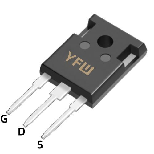
FETs are voltage-controlled devices with three terminals: source (S), gate (G), and drain (D). They operate using a single type of charge carrier (unipolar), either electrons (N-channel) or holes (P-channel) .
JFET (Junction FET):
A reverse-biased PN junction between the gate and channel modulates current flow. JFETs have high input impedance and low noise, making them ideal for RF applications .
MOSFET (Metal-Oxide-Semiconductor FET):
A metal-oxide layer isolates the gate, allowing voltage to induce a channel. MOSFETs are widely used in power electronics due to their low on-resistance (Rds(on)) and high switching speed. For instance, YFW’s YFW13003 NPN power transistor, with a 700V Vceo rating, is optimized for high-voltage switching in power supplies .
Transistor performance is defined by several critical parameters, which must align with application requirements.
Vceo (Collector-Emitter Voltage): The maximum voltage the collector-emitter junction can withstand. Exceeding this value may cause breakdown. YFW’s 2SC3265-Y NPN transistor has a Vceo of 30V, suitable for low-voltage circuits .
Vebo (Emitter-Base Voltage): The maximum reverse voltage across the emitter-base junction, typically lower than Vceo.
Ic (Collector Current): The maximum continuous current through the collector. YFW’s YFW13003 handles up to 1.5A, making it suitable for motor control .
Pd (Power Dissipation): The maximum power the transistor can dissipate without damage, calculated as Pd = Ic × Vce. High-power transistors like YFW’s 2SC3265-Y require heat sinks to manage thermal stress .
Rds (on) is the resistance between the drain and source when the MOSFET is fully 导通. Lower Rds (on) reduces power loss and improves efficiency. For example, YFW’s MOSFETs are designed with low Rds (on) to minimize heat generation in power converters .
Transistors must operate within specified temperature ranges. YFW’s products, such as the 2SA1013, are rated for temperatures up to 150°C, ensuring reliability in harsh environments .
Transistors are integral to various industries:
Consumer Electronics: BJTs amplify audio signals in speakers, while MOSFETs enable efficient power management in smartphones.
Industrial Control: High-voltage transistors like YFW13003 drive motors and inverters in factory automation .
Automotive Systems: FETs with fast switching speeds are used in EV chargers and engine control units.
Future Innovations:
Wide Bandgap Materials: Gallium nitride (GaN) and silicon carbide (SiC) transistors offer higher efficiency and power density, suitable for next-gen power electronics .
3D Stacking: Advanced packaging techniques, such as FinFETs, enhance transistor density and performance .
Transistors, with their ability to amplify and switch signals, remain indispensable in modern technology. YFW’s commitment to innovation ensures its transistors meet rigorous standards, offering high reliability and performance across diverse applications. By understanding their working principles and key parameters, engineers can select the optimal transistor for their designs, driving advancements in electronics and beyond.