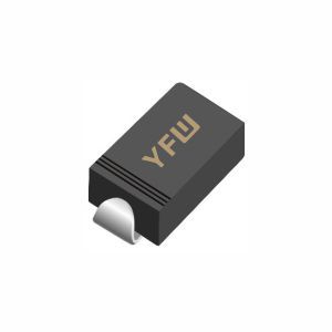
A Zener diode consists of a heavily doped PN junction, creating a narrow depletion region. When forward-biased, it behaves like a regular diode, allowing current flow once the forward voltage exceeds the threshold (≈0.7V for silicon). However, its defining characteristic lies in reverse bias operation. As the reverse voltage increases, the electric field across the depletion region intensifies. At a specific voltage—known as the Zener voltage (Vz)—the diode enters the reverse breakdown region, enabling controlled current flow.
The reverse breakdown in Zener diodes can occur through two mechanisms:
Zener Breakdown:
This quantum mechanical effect dominates at lower voltages (typically <5V). The strong electric field in the narrow depletion region causes electrons to tunnel directly from the valence band to the conduction band, generating electron-hole pairs. This process is temperature-independent and results in a sharp breakdown voltage.
Avalanche Breakdown:
At higher voltages (>5V), the electric field accelerates minority carriers, which collide with atoms to generate additional carriers via impact ionization. This cascading effect, akin to an avalanche, leads to a rapid increase in current. Unlike Zener breakdown, avalanche breakdown is temperature-dependent, with breakdown voltage increasing slightly with temperature.
In practical Zener diodes, especially those with Vz between 5V and 8V, both mechanisms coexist, creating a hybrid breakdown 特性.
The key utility of Zener diodes lies in their ability to stabilize voltage. When connected in parallel with a load in reverse bias, the diode maintains a nearly constant voltage across its terminals, even as the input voltage or load current fluctuates. Here’s how it works:
Below Vz: The diode blocks reverse current, and the load operates at the input voltage.
At Vz: The diode enters breakdown, shunting excess current to maintain the output voltage at Vz.
Above Vz: The diode conducts heavily, preventing the voltage from rising further and protecting downstream components.
This self-regulating behavior makes Zener diodes ideal for voltage reference circuits, surge protection, and power supply stabilization.
Manufacturers like YFW provide detailed specifications to ensure optimal performance:
Zener Voltage (Vz): The target voltage at which breakdown occurs, available in a wide range (e.g., YFW’s SMA2Z10A offers 10V~10.5V).
Power Dissipation (Pz): The maximum power the diode can handle without damage (e.g., 2W for SMA2Z10A).
Dynamic Impedance (Zz): A measure of voltage stability; lower Zz indicates better regulation.
Temperature Coefficient: Accounts for voltage drift with temperature, critical for precision applications.
Zener diodes find widespread use in diverse industries:
Voltage Regulation:
They serve as shunt regulators in power supplies, ensuring a stable output voltage despite input variations. YFW’s BZT52C series, available in SOD-123 and SOD-323 packages, is well-suited for compact designs.
Overvoltage Protection:
By clamping voltage spikes, they safeguard sensitive components in automotive electronics, industrial equipment, and consumer devices.
Signal Conditioning:
In clipping circuits, Zener diodes limit signal amplitudes, preventing damage to analog components.
Temperature Sensing:
Their voltage-temperature relationship enables use in temperature-compensated circuits.
Zener diodes exemplify the marriage of semiconductor physics and practical engineering. By leveraging reverse breakdown, they deliver reliable voltage regulation and protection, empowering innovations in electronics. YFW’s portfolio of Zener diodes, including surface-mount and through-hole variants, underscores their commitment to precision and durability, catering to applications from low-power electronics to high-voltage systems. As the semiconductor industry evolves, Zener diodes remain a vital component, ensuring stability and efficiency in an increasingly connected world.
