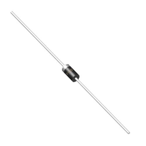
The body diode’s reverse recovery is a critical bottleneck. The large PN junction area in SJ structures leads to excessive minority carrier storage during forward conduction, resulting in high Qrr and trr . When the diode switches off, the sudden depletion of stored charges causes voltage overshoots and oscillations, increasing EMI and risking device failure under repetitive hard commutation . Additionally, the trade-off between RDS(on) and reverse recovery softness complicates design optimization, as thicker n− buffer layers reduce Qrr but compromise on-resistance .
YFW addresses these challenges through a multi-faceted approach:
By introducing an n+/n−-buffer layer between the drift region and substrate, YFW’s SJ MOSFETs mitigate reverse recovery issues. This layer acts as a carrier reservoir, maintaining current continuity during the reverse recovery phase and suppressing voltage spikes . Simulations show that a 10-μm n+ buffer layer with impurity concentrations between 4×10¹⁵ cm⁻³ and 6×10¹⁶ cm⁻³ reduces overshoot voltage by <20 V while limiting RDS(on) increase to <5% .
YFW employs electron irradiation (ER) and heavy-metal doping to create recombination centers in the drift region. This accelerates carrier recombination during reverse recovery, drastically reducing Qrr and improving softness . For example, YFW’s αMOS5™-based SJ MOSFETs achieve Qrr reductions of up to 30% compared to conventional designs, minimizing switching losses in half-bridge and LLC converter topologies .
YFW’s patented dual PW (p-well) and pillar architecture optimizes carrier injection efficiency during forward conduction. This design, combined with small-dimension contact etching, balances low Vf (forward voltage) and fast recovery, ensuring robust performance in high-current applications like EV fast chargers .
YFW’s optimized SJ MOSFETs demonstrate exceptional results in real-world scenarios:
Reverse Recovery Robustness: Tested at 50A forward current and 1000A/μs di/dt, YFW’s AOK042A60FD variant shows minimal voltage overshoot (<900V) and suppressed oscillation, outperforming competitors in bridge applications .
Efficiency Gains: In 40kW EV charging modules, YFW’s SJ MOSFETs achieve 96.28% efficiency with balanced thermal performance (65°C vs. 64.9°C for imported alternatives) .
Reliability: Conservative termination designs evenly distribute electric fields, preventing localized hotspots during reverse recovery and extending device lifespan .
YFW’s advancements in body diode optimization redefine SJ MOSFET performance, addressing the critical challenges of reverse recovery while maintaining low
RDS(on) and high-frequency capabilities. By integrating buffer layer engineering, carrier lifetime control, and structural innovations, YFW delivers devices that enable higher power density, efficiency, and reliability in applications ranging from renewable energy systems to industrial drives. For tailored solutions, contact YFW at
www.yfwdiode.com.
This article highlights YFW’s commitment to pushing the boundaries of power semiconductor technology. Stay tuned for future updates on our latest innovations
