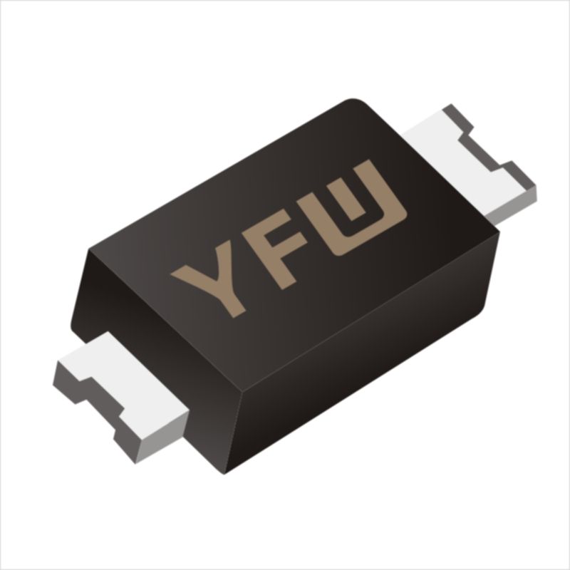
The choice of semiconductor material directly impacts carrier mobility and breakdown characteristics. Silicon (Si) remains widely used due to its cost-effectiveness, but silicon carbide (SiC) offers superior performance for high-speed scenarios. SiC exhibits a breakdown field strength ~10× higher than Si (2.8 MV/cm vs. 0.3 MV/cm) and improved thermal conductivity, enabling faster carrier transport and reduced thermal runaway risks. For instance, SiC-based avalanche diodes can sustain higher electric fields without premature breakdown, minimizing carrier transit time.
The physical architecture of the PN junction plays a pivotal role:
Depletion Layer Thickness: A narrower depletion layer reduces carrier transit time but must balance breakdown voltage requirements. YFW’s designs employ precision etching to achieve sub-micron depletion layers, enhancing speed while maintaining stability.
Doping Profile: Optimized doping concentrations in the avalanche region (e.g., low-doped drift layers) ensure uniform electric fields, preventing localized premature breakdown and minimizing gain-bandwidth trade-offs.
Avalanche multiplication introduces a fundamental trade-off: higher gain (M) often leads to slower response due to increased carrier multiplication time. The GBP, defined as \(\text{GBP} = M \times \text{Bandwidth}\), imposes a ceiling on performance. Modern avalanche photodiodes (APDs) achieve GBP values exceeding 1 THz through engineered electric field distributions and resonant avalanche effects. YFW’s APDs leverage this principle to maintain high gain (9–19.5) while delivering 53 GHz bandwidth, ensuring rapid signal processing in fiber-optic systems.
Temperature fluctuations affect carrier mobility and breakdown voltage. Higher temperatures increase lattice scattering, reducing electron velocity and extending transit time. For example, a 50°C rise in Si-based diodes can decrease mobility by ~30%, slowing response. YFW integrates active thermal stabilization (e.g., Peltier coolers) to maintain operating temperatures within ±0.1°C, ensuring consistent performance across diverse environments.
The diode’s interaction with external circuitry is critical:
Load Capacitance: Large capacitances (e.g., parasitic C in PCB layouts) prolong charging/discharging times. YFW’s devices feature low junction capacitance (<1 pF) and optimized package designs to mitigate this effect.
Reverse Recovery Time: Fast switching requires minimizing reverse recovery current. YFW’s avalanche diodes achieve <300 ns reverse recovery time through epitaxial layer engineering and edge termination techniques.
Defects in crystal growth or processing degrade uniformity and speed. For example, micro-pipes in SiC wafers reduce blocking voltage and increase leakage currents. YFW employs advanced inspection systems (e.g., confocal tomography) to detect sub-micron defects during production, ensuring >99% yield for high-speed applications.
YFW’s avalanche diodes exemplify the marriage of material science, structural innovation, and process control. By addressing factors like material selection, GBP optimization, and thermal stability, YFW delivers devices that excel in demanding high-speed environments. For applications requiring nanosecond-level response (e.g., 112 Gbps optical links), YFW’s solutions offer unmatched reliability and performance, setting benchmarks for next-generation avalanche diode technology.
For cutting-edge avalanche diode designs, visit YFW Diodes 