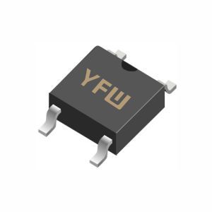
A PN junction consists of a P-type semiconductor (rich in holes) and an N-type semiconductor (abundant in electrons). When combined, these form a depletion region with an inherent electric field that prevents further charge carrier diffusion under equilibrium conditions . Forward biasing (connecting P to positive and N to negative) reduces the depletion layer, allowing current flow, while reverse biasing (opposite connection) widens the layer, blocking current except for a tiny leakage .
The most common type, standard PN diodes are used for rectification, converting alternating current (AC) to direct current (DC). They exhibit a distinct forward voltage drop (e.g., ~0.7V for silicon) and high reverse breakdown voltage, making them ideal for power supply applications . YFW’s high-voltage diodes are engineered to handle demanding scenarios, ensuring reliability in industrial and automotive systems.
Designed to operate in reverse breakdown without damage, Zener diodes are crucial for voltage regulation. Their unique doping profile allows them to maintain a stable voltage across their terminals, even with varying currents . YFW’s Zener diodes, such as the MM1W165, offer precise voltage clamping, protecting sensitive circuits in consumer electronics and medical devices.
Unlike traditional PN junctions, Schottky diodes feature a metal-semiconductor junction, resulting in lower forward voltage drop (e.g., ~0.3V) and faster switching speeds. These attributes make them suitable for high-frequency applications like switching power supplies . YFW’s SBD series, including the SS34, delivers low power loss and high efficiency, catering to energy-conscious designs.
Optimized for rapid switching, FRDs minimize reverse recovery time (TRR), critical in PWM (pulse-width modulation) circuits and motor drives. YFW’s SF36 FRD, with a TRR of 35ns, ensures smooth operation in renewable energy inverters and electric vehicles .
A specialized PN junction diode, LEDs emit light when forward biased. YFW’s LED solutions, integrated into smart lighting systems, combine energy efficiency with long lifespan, aligning with global sustainability goals .
PN junctions can be fabricated using various methods:
Diffusion: The most common technique, where impurities are introduced into the semiconductor substrate through high-temperature exposure .
Alloying: A metal pellet is fused with the semiconductor to form the junction, suitable for high-current applications .
Epitaxy: Thin layers of doped semiconductor materials are grown on a substrate, enabling precise control over junction characteristics.
YFW employs advanced diffusion and epitaxy processes to ensure consistent quality across its diode portfolio, including rectifier bridges and MOSFETs, which are vital for power management in industrial equipment .
PN junction diodes are ubiquitous in:
Consumer Electronics: Rectifiers in chargers, LEDs in displays.
Automotive: Voltage regulators in ECUs, FRDs in motor control.
Renewable Energy: Inverters for solar panels, Schottky diodes in wind turbines.
Medical Devices: Precision voltage clamping in diagnostic equipment.
YFW’s commitment to innovation ensures its diodes meet stringent industry standards, such as AEC-Q101 for automotive applications, providing customers with reliable, high-performance solutions .
From standard rectifiers to advanced Schottky and fast recovery diodes, PN junction diodes underpin modern electronics. YFW’s comprehensive range, backed by cutting-edge manufacturing and rigorous testing, addresses diverse market needs while prioritizing efficiency and durability. By leveraging the unique properties of PN junctions, YFW continues to drive progress in semiconductor technology, empowering industries worldwide.
