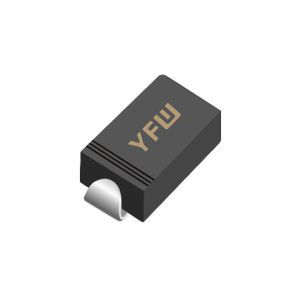
Yes, most standard MOSFETs feature a parasitic body diode (also known as an intrinsic or anti-parallel diode) formed by the PN junction between the device’s source (S) and drain (D) terminals. This diode is an integral part of the MOSFET’s structure, particularly in discrete devices. For example, in an N-channel MOSFET, the source and drain are N-type semiconductors, while the substrate (body) is P-type. When the source is connected to the body (a common configuration), the body diode acts as a reverse-biased PN junction between the drain and source. This diode allows current to flow from the drain to the source when the MOSFET is off, but blocks it in the opposite direction when the device is on.
However, there are exceptions. Some specialized MOSFETs, such as those using Silicon-on-Insulator (SOI) technology or certain four-pin packages (where the body is isolated), may eliminate the body diode. These designs are rare and typically reserved for applications requiring bidirectional current control or precise voltage blocking.
The body diode plays a critical role in power electronics, particularly in switching and protection:
The body diode prevents damage from accidental reverse voltage application across the MOSFET. If the drain voltage becomes negative relative to the source (e.g., due to inductive loads or power supply reversals), the diode conducts, diverting the current and safeguarding the device.
In switching applications like
DC-DC converters or motor drives, inductive loads generate back EMF (electromotive force) when the MOSFET turns off. The body diode provides a
freewheeling path for the inductive current, preventing voltage spikes that could otherwise damage the MOSFET or adjacent components. For instance, in a buck converter, the body diode of the low-side MOSFET conducts during the dead time between switching cycles, ensuring continuous current flow through the inductor .
The body diode eliminates the need for an external freewheeling diode in many applications, reducing component count and cost. However, its limitations (e.g., higher forward voltage drop and slower recovery compared to dedicated diodes) may necessitate external Schottky diodes in high-frequency or high-efficiency designs .
In power MOSFETs, a parasitic bipolar junction transistor (BJT) exists between the drain and source. The body diode helps suppress BJT latch-up by shorting the base-emitter junction, ensuring stable operation under extreme conditions .
While the body diode offers critical benefits, its characteristics can impact circuit performance:
Reverse Recovery Loss: When the body diode turns off, stored charge (Qₙₙ) causes reverse recovery current, leading to energy losses and voltage overshoots. This is particularly problematic in high-frequency applications. YFW’s MOSFETs, such as the 7N65AF (650V, 7A) with a reverse recovery time (tᵣᵣ) of 19 ns , are optimized to minimize these losses.
Forward Voltage Drop: The body diode’s forward voltage (Vբ) is typically higher than that of Schottky diodes, increasing conduction losses. For example, YFW’s MBR6060PTS Schottky diode (60V, 30A) features a Vբ of 0.63V , making it ideal for replacing body diodes in low-voltage applications.
At YFW, we design MOSFETs with advanced features to address body diode limitations:
Low Reverse Recovery Charge (Qₙₙ): Our superjunction (SJ) MOSFETs, such as the YFW10N65AF (650V, 10A), leverage optimized doping profiles to reduce Qₙₙ, enhancing efficiency in high-frequency switching .
Fast Switching Speed: Devices like the YFW8N65AF (650V, 8A) with a tᵣᵣ of 25.1 ns enable rapid transitions, minimizing switching losses.
Integrated Protection: YFW’s MOSFETs incorporate robust body diodes to handle inductive transients, ensuring reliability in motor control and power supply applications.
The body diode is a fundamental component of most MOSFETs, providing reverse voltage protection, freewheeling capabilities, and simplified circuit design. While its limitations require careful consideration in high-performance applications, YFW’s MOSFETs are engineered to balance functionality and efficiency. By combining low Qₙₙ, fast switching speeds, and integrated protection, our devices empower engineers to design reliable, high-frequency power systems.
For technical specifications or custom solutions, explore YFW’s MOSFET portfolio at
www.yfwdiode.com or contact our team for tailored support.
