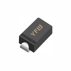
Understanding MOSFET Switching Characteristics for Efficient Power Management
Date:2025-05-05 Categories:Product knowledge Hits:747 From:Guangdong Youfeng Microelectronics Co., Ltd
MOSFETs (Metal-Oxide-Semiconductor Field-Effect Transistors) act as voltage-controlled switches, offering near-instantaneous on/off operation with minimal power loss. Unlike bipolar junction transistors (BJTs), MOSFETs rely on electric fields rather than minority carrier injection, enabling faster switching speeds and lower gate drive requirements .
RDS(ON): The drain-source on-resistance determines conduction losses. YFW’s YFW50N03AD features an ultra-low 5.8 mΩ RDS(ON) , reducing power dissipation in high-current applications.
Gate Charge (Qg): Influences switching speed. The YFW15G04S achieves Qg = 43 nC (typical), ensuring rapid transitions and low gate drive power .
Switching Speed: MOSFETs operate in nanosecond ranges, with rise/fall times (Tr/Tf) as low as 10–100 ns .
Delay Time (td(on)): The gate voltage (VGS) rises to the threshold voltage (VTH), initiating channel formation.
Rise Time (Tr): VGS exceeds VTH, allowing drain current (ID) to increase while drain-source voltage (VDS) remains high.
Miller Plateau: VGS plateaus as the Miller capacitance (CGD) discharges, causing VDS to drop rapidly .
Final Charging: VGS reaches its maximum value, minimizing RDS(ON) .
Delay Time (td(off)): VGS decreases to the Miller plateau voltage, maintaining ID.
Fall Time (Tf): VDS rises as ID decreases, driven by the load.
Final Discharge: VGS drops below VTH, fully turning off the device .
YFW’s
YFW50N03AD (30V, 50A) and
YFW15G04S (40V, 18A) leverage trench technology to achieve industry-leading RDS(ON) values, ideal for high-frequency
DC-DC converters and motor drives .
With minimized gate charge and parasitic capacitances, YFW MOSFETs reduce switching losses. For example, the YFW15G04S supports PWM frequencies up to 200 kHz, critical for compact power supply designs .
YFW devices undergo rigorous avalanche testing and feature extended safe operating areas (SOA), ensuring reliability in harsh environments .
Gate Drive Circuit: Use dedicated drivers (e.g., YFWGD101) to provide sufficient current for rapid VGS transitions .
Snubber Circuits: Mitigate voltage spikes during turn-off to protect the MOSFET.
Thermal Management: Proper heat sinking is essential for high-power applications to prevent thermal runaway.
YFW MOSFETs excel in:
Consumer Electronics: Battery management systems and fast-charging adapters.
Automotive: Electric vehicle (EV) inverters and LED lighting.
Industrial: Solar inverters and motor control units.
Mastering MOSFET switching characteristics is vital for designing efficient power systems. YFW Microelectronics combines cutting-edge technology with meticulous engineering to deliver MOSFETs that balance low RDS(ON), fast switching, and robust reliability. Explore our YFW50N03AD and YFW15G04S series today to elevate your next project’s performance.

Previous:
Classification, Structure, and Principle of MOSFET
Next:
Understanding the Conduction Conditions of P-Channel MOSFETs