
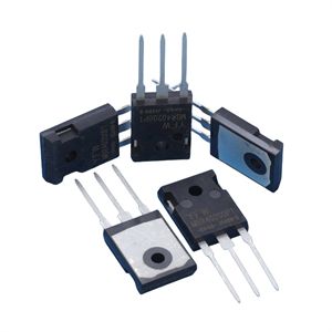
Date:2024-09-26 Categories:Product knowledge Hits:630 From: Guangdong Youfeng Microelectronics Co., Ltd(YFW)
Schottky diodes have low resistance under forward voltage and are in a conducting state, equivalent to a turned on switch; Under the action of reverse voltage, the resistance is very large and in a cut-off state, like a disconnected switch. By utilizing the switching characteristics of Schottky diodes, various logic circuits can be formed. Due to the unidirectional conductivity of Schottky diodes, the PN junction conducts under positive bias, and the resistance in the conducting state is very small, about tens to hundreds of ohms; Under reverse bias, it is in a cut-off state and has a high resistance. Generally, silicon Schottky diodes have a resistance of over 10 Μ Ω, and germanium diodes have a resistance of tens to hundreds of kiloohms. By utilizing this characteristic, Schottky diodes will play a role in controlling the current on or off in circuits, making them an ideal electronic switch.
The most basic switch circuit, in which the two ends of the Schottky diode are connected to VCC and GND through resistors, respectively. The Schottky diode is in a reverse biased state and will not conduct. The AC voltage applied through point C1 cannot pass through the Schottky diode, and the AC component cannot be detected after point C2.
The connection of the Schottky diode is opposite to that shown in the figure. A Schottky diode in forward conduction state can allow the AC signal applied to point C1 to pass through the Schottky diode and be presented at the output of point C2. This is the state when the diode is conducting, also known as the "conducting" state of the switch.
This is the simplest circuit that adjusts the conduction state of Schottky diodes through the state of DC bias. Thus achieving control over communication signals. In practical applications, it is usually necessary to ensure that the voltage level on one side remains constant while adjusting the voltage level on the other side, in order to control the conduction of the diode. In RF circuits, this design often adds measures to prevent RF components from entering the logic/power supply lines on the biased lines to reduce interference, but overall, this design is still very common.
Previous: Classification, Structure, and Principle of MOSFET
Next: Using voltage inspection method to quickly locate fault points in integrated circuits
