
Date:2026-03-03 Categories:Product knowledge Hits:1758 From:Guangdong Youfeng Microelectronics Co., Ltd
Bipolar transistor amplifier circuit, common-base amplifier circuit, common-collector amplifier circuit
Those who have studied analog electronics should be familiar with the amplifier circuits of triode or field-effect transistors (all amplifier circuits mentioned in this article refer to voltage amplification). This is a key point in analog electronics, but also a difficult one. It's important to know, but it's hard to understand how it works. No worries, this time I will take the three configurations of triode amplifier circuits as an example to briefly explain the calculation formula for the amplification factor of amplifier circuits.
The basic configuration amplifier circuits composed of bipolar junction transistors (BJTs) can be divided into three types: the common-emitter amplifier circuit, the common-base amplifier circuit, and the common-collector amplifier circuit.
1. Common-emitter amplifier circuit
The circuit schematic is as follows: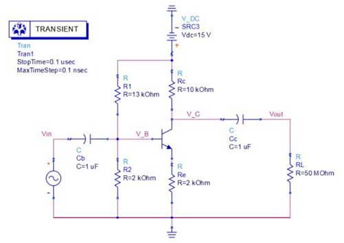
①. The amplification factor is: A=-Rc/Re. The values of Rc and Re are designed according to the requirements. ②. Input impedance: Zin = beta * Re. (R1 and R2 provide bias voltage for the transistor, which is ignored here for simplicity, but should be considered in practice.) Due to the circuit amplification characteristics of the transistor, Re needs to be amplified by beta times when converted to the input terminal, resulting in a high input impedance. ③. Output impedance: Zout = Rc. To reduce the current of the transistor and lower power consumption, Rc is generally set to a large value. ④. Frequency characteristics: Due to the Miller effect, the parasitic capacitance between the base and collector of the transistor in the amplification region will be amplified by A times and reflected to the input terminal, resulting in poor frequency characteristics and an inability to amplify high-frequency signals.
2. Common-collector amplifier circuit
The input resistance of the common-collector amplifier circuit is large, while the output resistance is small. However, it only has current amplification capability and no voltage amplification capability, generally close to but less than 1. The AC path of the common-collector amplifier circuit is as follows.
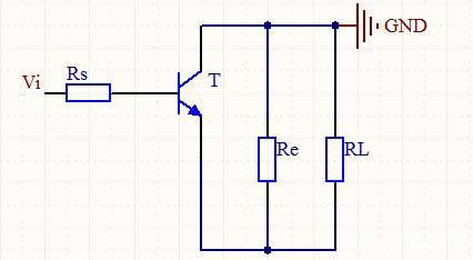
At first glance, it seems similar to a common-collector amplifier circuit where the emitter has no resistance. The difference lies in the location of the AC ground. You can compare the two to better distinguish them. The formula for AC amplification is: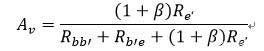
From the formula, it can be seen that the voltage amplification factor cannot be greater than 1. Usually, 1 + β is large, and multiplied by a large resistor Re', so the result is close to 1. In this formula, only Re' is different from the formulas of the above two amplification circuits. Its value is equal to Re in parallel with R L. The meanings of other letters are the same as above.
3. Common-base amplifier circuit
The input resistance of a common-base amplifier circuit is very small, while its output resistance is very large, and it has good frequency characteristics. However, a common-base amplifier circuit only has voltage amplification capability and does not have current amplification capability. Let's take a direct look at the AC circuit diagram.
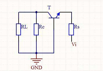
Does this circuit look strange? The common-base amplifier circuit has a current flowing from the emitter to the collector (the current direction itself feels strange, but it is indeed like this). I believe everyone should be familiar with the four components on the schematic diagram through the introduction of the common-emitter circuit. Let's directly look at the formula for this circuit: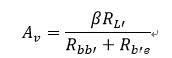
In fact, the magnitude of this voltage amplification factor is the same as that when the emitter of the common-emitter amplifier circuit is not connected to a resistor, except for a negative sign difference between the two. The meaning of each letter in the formula is also the same as that in the common-emitter amplifier circuit, that is, β represents the amplification factor of the transistor, R L' equals R c in parallel with R L, R b b' is composed of the base lead resistance and the base region body resistance, and the calculation method of R b'e is also the same as that in the common-emitter amplifier circuit.
How to distinguish the three working states of a transistor
In simple terms, the operational state of a transistor can be determined by the magnitude of Uce. When Uce is close to the supply voltage VCC, the transistor operates in the cut-off state. The cut-off state means that the transistor is essentially non-functional, with a small Ic current (approximately zero). Therefore, since no current flows through R2, its voltage approaches 0V, and thus Uce approaches the supply voltage VCC.
If Uce is close to 0V, the transistor operates in saturation state. What is saturation state? It means that the Ic current has reached its maximum value, and even if Ib increases, it cannot increase further.
The above two states are generally referred to as the switch state. Besides these two, the third state is the amplification state, where the measured Uce is generally close to half of the power supply voltage. If the measured Uce is biased towards VCC, the transistor tends towards the cut-off state; if it is biased towards 0V, the transistor tends towards the saturation state.
Stable operation principle of amplifier circuit
1: Due to the increase in temperature, the collector current Ic increases, leading to an increase in the emitter current Ie. Consequently, the voltage across R4, IeR4, also increases. Ub is provided by the voltage divider resistor and remains essentially unchanged. Since Ube = Ub - IeR4, Ube decreases, which in turn reduces the corresponding base current Ib. This suppresses the increase in collector current Ic, stabilizing the DC operating point of the collector current and thus mitigating the adverse effects of temperature rise on the circuit.
2: R4 is a key component in the feedback resistor amplifier circuit. By appropriately increasing the resistance of R4, the feedback becomes stronger, leading to better stability. Therefore, it is necessary to make reasonable choices based on the actual circuit design. To reduce the loss of AC energy in R4, a capacitor C3 is added to bypass the AC to ground, which can enhance the AC gain of the amplifier circuit.
3: The current negative feedback bias circuit exhibits excellent temperature stability. By selecting appropriate bias resistor values and designing a reasonable DC operating point, the amplifier circuit can operate stably and reliably. Therefore, it is a widely used bias circuit in amplifier circuits.
If one wishes to effectively utilize a transistor, it is imperative to master the aforementioned three basic configuration amplifier circuits
Previous: Classification, Structure, and Principle of MOSFET
Next: Characteristics and parameters of high-frequency rectifier diode
