Date:2025-07-15 Categories:Product knowledge Hits:1070 From:Guangdong Youfeng Microelectronics Co., Ltd
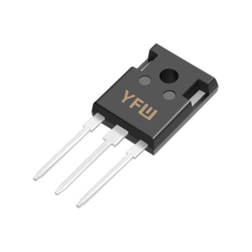
The packaging form and pin identification of transistors
The commonly used packaging forms of transistors include metal packaging and plastic packaging, and the arrangement of pins follows certain rules,
Place the bottom view position so that the three pins form the vertices of an isosceles triangle, with ebc from left to right; For small and medium power plastic transistors, place the plane facing themselves and the three pins facing downwards according to the diagram, and the EBC is from left to right.
At present, there are many types of transistors in China with different pin arrangements. For transistors with uncertain pin arrangements during use, measurements must be taken to determine the correct position of each pin, or the transistor user manual must be consulted to clarify the characteristics and corresponding technical parameters and information of the transistor.
The current amplification effect of transistor
The transistor has a current amplification function, which essentially means that the transistor can control the large change in collector current with a small change in base current. This is the most fundamental and important characteristic of a transistor. We refer to the ratio of Δ Ic/Δ Ib as the current amplification factor of the transistor, denoted by the symbol "β". The current amplification factor is a constant value for a certain transistor, but it may also change with the variation of the base current during the operation of the transistor.
Three working states of transistor
Cut off state: When the voltage applied to the emitter junction of the transistor is less than the conduction voltage of the PN junction, the base current is zero, and the collector current and emitter current are both zero. At this point, the transistor loses its current amplification function, and the gap between the collector and emitter is equivalent to the open state of the switch. We call the transistor in the cut off state.
Amplification state: When the voltage applied to the emitter junction of the transistor is greater than the conduction voltage of the PN junction and is at an appropriate value, the emitter junction of the transistor is forward biased and the collector junction is reverse biased. At this time, the base current controls the collector current, making the transistor have a current amplification effect. The current amplification factor β=Δ Ic/Δ Ib, and the transistor is in an amplification state.
Saturated conduction state: When the voltage applied to the emitter junction of a transistor is greater than the conduction voltage of the PN junction, and when the base current increases to a certain extent, the collector current no longer increases with the increase of the base current, but remains relatively stable near a certain value. At this point, the transistor loses its current amplification function, and the voltage between the collector and emitter is very small. The collector and emitter are equivalent to the conduction state of a switch. The state of a transistor is called saturation conduction state.
Based on the high or low potential of each electrode during the operation of a transistor, the working state of the transistor can be determined. Therefore, electronic maintenance personnel often use a multimeter to measure the voltage of each pin of the transistor during maintenance, in order to determine the working condition and status of the transistor.
Using a multimeter to detect transistors
Discrimination of transistor base: According to the schematic diagram of the transistor structure, we know that the base of the transistor is the common pole of the two PN junctions in the transistor. Therefore, when discriminating the base of the transistor, we only need to find the common pole of the two PN junctions, which is the base of the transistor. The specific method is to adjust the multimeter to the resistance mode of R × 1k, first place the red probe on one pin of the transistor, and touch the other two pins of the transistor with the black probe. If both are turned on, the pin where the red probe is placed is the base of the transistor. If it cannot be found once, switch the red probe to the other pin of thetransistor and test again twice; If you haven't found it yet, replace the red probe and test again twice. If it is not found yet, use a black probe to place it on one of the pins of the transistor, and use a red probe to test twice to see if it is fully connected. If it fails once, replace it. This way, at most 12 times, the base can always be found.
Discrimination of transistor types: There are only two types of transistors, PNP and NPN. When discriminating, it is only necessary to know whether the base is a P-type material or an N-type material. When using a multimeter in the R × 1k range, the black probe represents the positive pole of the power supply. If the black probe conducts when connected to the base, it indicates that the base of the transistor is made of P-type material, and the transistor is of NPN type. If the red probe is connected to the base and conducts, it indicates that the base of the transistor is made of N-type material, and the transistor is of PNP type
Crystal transistor is one of the basic semiconductor components, which has the function of current amplification and is the core component of electronic circuits. A transistor is made by fabricating two PN junctions that are very close to each other on a semiconductor substrate. The two PN junctions divide the positive block semiconductor into three parts, with the middle part being the base region and the two sides being the emitter and collector regions. There are two arrangements: PNP and NPN,
Lead out corresponding electrodes from three regions, namely base b, emitter e, and collector c.
The PN junction between the emitter region and the base region is called the emitter junction, and the PN junction between the collector region and the base region is called the collector junction. The base region is very thin, while the emitter region is thick with high impurity concentration. The PNP transistor emitter region "emits" holes, which move in the same direction as the current direction, so the emitter arrow points inward; The emitter region of an NPN transistor emits free electrons, which move in the opposite direction to the current direction, so the emitter arrow is pointing outward. The emitter arrow is pointing outward. The direction of the emitter arrow is also the conduction direction of the PN junction under forward voltage. Both silicon transistor and germanium transistor have two types: PNP and NPN.
Previous: Classification, Structure, and Principle of MOSFET
Next: The structure, function, and working principle of a transistor