Date:2025-06-23 Categories:Product knowledge Hits:1016 From:Guangdong Youfeng Microelectronics Co., Ltd
The silicon phototransistor is a BT138-600E photoelectric conversion device that utilizes the photoelectric effect to convert optical signals into electrical signals. It has the characteristics of simple structure, high sensitivity, and fast response speed, and is widely used in fields such as optoelectronic detection, communication, and optoelectronic measurement.
1、 Basic structure:
The structure of a silicon phototransistor is basically similar to that of a regular silicon transistor, mainly composed of a PN structure. Among them, the emitter is a P-type region, the collector is an N-type region, and the base is a P-type or N-type region. The formation of PN structure enables silicon phototransistors to convert optical signals into electrical signals.
2、 Advantages and disadvantages:
silicon phototransistors have the following advantages:
1. High sensitivity: silicon phototransistors are very sensitive to light signals and can detect very small light signals.
2. Fast response speed: The response speed of silicon phototransistors can reach microsecond level, suitable for high-speed photoelectric detection.
3. Good reliability: silicon phototransistors have the characteristics of long lifespan, stability, and reliability.
4. Economical and practical: The manufacturing cost of silicon phototransistors is relatively low.
The disadvantages of silicon phototransistors include:
1. High noise: silicon phototransistors generate certain noise signals during operation.
2. Poor wavelength selectivity: silicon phototransistors have poor wavelength selectivity and can only receive optical signals within a certain wavelength range.
3. Temperature has a significant impact: the performance of silicon phototransistors is easily affected by temperature.
3、 Working principle:
The working principle of silicon phototransistorr is based on the photoelectric conversion principle of PN junction. When light is irradiated onto the photosensitive electrode, photon energy causes electrons in the photosensitive electrode to transition from the valence band to the conduction band, while generating holes. These electrons and holes are the charge carriers in the photosensitive electrode.
In the case of forward bias, electrons in the photosensitive electrode will be pushed towards the base region, while holes will be pushed towards the emitter region. Due to the voltage between the base and emitter, electrons will form a current between the base region and the emitter, and generate an output signal at the emitter.
4、 Application:
silicon phototransistors are widely used in the following fields:
1. Optoelectronic detection: silicon phototransistors can be used for receiving and detecting optical signals, such as photoelectric switches, photoelectric sensors, etc.
2. Communication: silicon phototransistors can be used as optical receivers in optical communication systems to receive and convert optical signals.
3. Optoelectronic measurement: silicon phototransistors can be used for measuring optical power and detecting optical intensity.
4. Other applications: silicon phototransistors can also be used in fields such as optical electron microscopy and optoelectronic computers.
5、 Identification method:
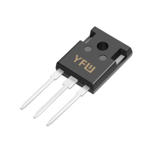
1. Appearance recognition: silicon phototransistors have a similar appearance to ordinary transistors, but their packaging is usually compact and comes in various forms such as TO-18, TO-92, SMD, etc. By examining its appearance, one can preliminarily determine its type and packaging form.
2. Pin identification: silicon phototransistors typically have three pins, namely the base (B), emitter (E), and collector (C). You can confirm the corresponding relationship of pins by referring to the data manual of the device or the labeling on the package.
3. Refer to the data manual: The data manual for silicon phototransistors includes detailed device parameters and performance indicators, such as photocurrent gain, photocurrent response speed, wavelength response range, etc. By consulting the data manual, one can further understand the characteristics of the device, in order to make the correct selection and application.
6、 Testing:
1. Prepare equipment and instruments: A digital voltmeter, a constant current source, and a multimeter probe are required.
2. Connection circuit: Connect the anode of the phototransistor to the positive pole of the constant current source, and connect the cathode to the positive pole of the digital voltmeter.
3. Setting current: By adjusting the current of the constant current source, the working state of the phototransistor can be changed. You can gradually increase the current and observe the reading on the digital voltmeter.
4. Measure voltage: Use a multimeter probe to connect the negative terminal to the cathode of the phototransistor and the positive terminal to the anode, and read the voltage value.
5. Analysis results: By observing the changes in voltage values, the working state and performance of the phototransistor can be determined. It should be noted that for the detection of silicon phototransistors, it is necessary to avoid exceeding their rated current and voltage to avoid damaging the device.
7、 Selection:
When selecting a silicon phototransistor, the following factors need to be considered:
1. Photocurrent gain: Choose the appropriate photocurrent gain according to application requirements. Generally speaking, the larger the photocurrent gain, the larger the output photocurrent signal. For applications that require high photosensitivity, devices with larger photocurrent gain can be selected.
2. Wavelength response range: Choose the appropriate wavelength response range according to the application needs. Different silicon phototransistors have varying degrees of response to light sources of different wavelengths, and appropriate devices need to be selected based on the wavelength of the light source in the application.
3. Packaging form: Choose the appropriate packaging form according to the space limitations and installation requirements of the application. There are multiple packaging forms available for silicon phototransistors, such as TO-18, TO-92, SMD, etc.
4. Performance indicators: Select appropriate performance indicators for silicon phototransistors based on application requirements, such as response speed, dark current, linear range, etc. Different applications have different requirements for these performance indicators, which need to be selected according to specific needs.
8、 Development history:
The development history of silicon phototransistors can be traced back to the 1950s. With the advancement of semiconductor technology, the performance of silicon phototransistors continues to improve, and their application fields are also expanding. At present, silicon phototransistors have been widely used in fields such as photoelectric sensing, optical communication, and photoelectric measurement. With the continuous improvement of people's requirements for the performance of optoelectronic devices, the development direction of silicon phototransistors mainly includes improving photoelectric conversion efficiency, reducing response time, expanding spectral response range, etc. Meanwhile, with the advancement of research and preparation technology for new materials, new optoelectronic devices such as nano phototransistors are gradually emerging and are expected to replace traditional silicon phototransistors in the future
Previous: Classification, Structure, and Principle of MOSFET