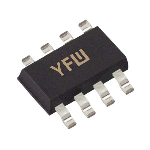
At the core of a photodiode lies a p-n junction or p-i-n structure, where a depletion region forms under reverse bias. When photons with energy exceeding the semiconductor’s bandgap strike the depletion layer, they generate electron-hole pairs through the photovoltaic effect. These carriers are separated by the electric field, creating a photocurrent proportional to the incident light intensity.
Photodiodes operate in two primary modes:
Photoconductive Mode: A reverse bias is applied to widen the depletion layer, reducing junction capacitance and enhancing response speed. This mode offers high linearity (current proportional to light power) and a broad dynamic range, making it ideal for applications requiring precision, such as optical receivers.
Photovoltaic Mode: No external bias is applied, relying solely on the built-in potential of the p-n junction. While this mode minimizes dark current, its nonlinear voltage response limits its use to low-light scenarios like solar cells.
The quantum efficiency (QE), defined as the ratio of generated electrons to incident photons, is a critical metric. High QE requires optimized material absorption and anti-reflective coatings to minimize surface reflection.
The p-i-n structure introduces an intrinsic (i) layer between p- and n-type regions, expanding the depletion layer for efficient light absorption. This design balances high quantum efficiency with fast response times, making PIN diodes suitable for high-speed data transmission in fiber optics. Their low dark current and linearity also favor applications like laser power monitoring and sensor arrays.
APDs leverage avalanche multiplication under high reverse bias. Incident photons generate primary carriers, which gain sufficient energy to ionize atoms, creating secondary electron-hole pairs. This cascading effect amplifies the photocurrent by factors of 10–100, enabling detection of ultra-weak signals in applications like lidar and quantum communication. However, APDs require precise voltage control to avoid breakdown and manage excess noise from the multiplication process.
Schottky diodes feature a metal-semiconductor junction, offering low forward voltage drop and fast switching. In photodetection, their wide depletion layer enhances sensitivity to shorter wavelengths (e.g., UV and visible light). These diodes are used in high-frequency applications like RF signal demodulation and optical sensors, where their low capacitance ensures minimal signal distortion.
Made from indium gallium arsenide, these diodes extend sensitivity into the near-infrared (NIR) and short-wave infrared (SWIR) ranges (800–2600 nm). Their high absorption coefficient and low dark current make them indispensable for telecom networks, spectroscopy, and night-vision systems. Advanced designs, such as SAM-APDs (separate absorption, grading, and multiplication), optimize performance by integrating InGaAs with InP for long-wavelength applications.
Silicon dominates visible and NIR detection (400–1100 nm). Its low dark current, high speed, and cost-effectiveness make it suitable for consumer electronics, solar cells, and general-purpose sensing. However, silicon’s bandgap limits its utility beyond 1100 nm.
Germanium extends sensitivity to 1600 nm but suffers from high dark current and slow response due to large parasitic capacitance. It is used in niche applications like mid-infrared spectroscopy and low-speed optical links.
InGaAs excels in the 1000–2600 nm range, critical for fiber-optic communications (1310 nm and 1550 nm) and industrial sensing. Its high electron mobility and compatibility with InP substrates enable high-speed, low-noise operation.
This alloy optimizes performance in the 1000–1350 nm range, balancing absorption efficiency and thermal stability. InGaAsP-based devices are widely used in telecom transmitters and receivers.
Graphene: While not yet mainstream, graphene-based photodetectors offer ultra-fast response (sub-picosecond) and broadband sensitivity. Their integration with silicon photonics holds promise for next-generation high-bandwidth applications.
Organic Materials: Organic photodiodes (OPDs) enable flexible, low-cost sensors for IoT and imaging. Recent advancements in heterojunction designs have improved their detectivity and stability, approaching commercial viability.
Photodiodes are versatile devices whose performance hinges on material selection and structural design. Silicon remains the workhorse for visible and NIR applications, while InGaAs and InGaAsP dominate long-wavelength scenarios. APDs and Schottky diodes address specialized needs for sensitivity and speed, respectively. As materials science evolves—with breakthroughs in graphene and organic semiconductors—the photodiode landscape continues to expand, driving innovation in photonics and sensing technologies. By understanding these mechanisms and advancements, engineers can select the optimal device for their specific application, ensuring efficiency and reliability in modern optical systems
