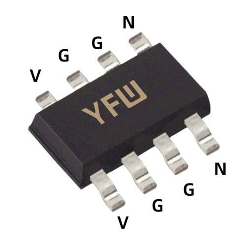
Traditional photodiodes, while widely used in applications ranging from light detection to optical communication, suffer from inherent drawbacks. Their reliance on external bias circuits for signal conversion not only increases system complexity but also limits bandwidth and scalability. For instance, conventional photodiodes in optical communication systems require discrete components to modulate light intensity or detect signals, leading to bulky architectures and reduced efficiency .
The Three-Electrode Optoelectronic PN Junction
Diode eliminates these inefficiencies by integrating a
Metal-Oxide-Semiconductor (MOS) structure directly into the device. By introducing a third electrode on the p-type region, this design enables dynamic control of carrier transport through an external electric field, fundamentally altering the diode’s optoelectronic behavior . This innovation allows the diode to function as both a
tunable light emitter and a
multifunctional photodetector within a single compact package, reducing the need for external circuitry and enhancing system integration.
The Three-Electrode
Diode features a vertically stacked structure, combining a traditional PN junction with a MOS capacitor. The p-type region, sandwiched between the n-type layer and the MOS gate, serves as the active zone for carrier modulation. When operated as a light emitter:
The third electrode applies a voltage to the MOS gate, altering the electric field in the p-type region. This modulates the recombination rate of electron-hole pairs, thereby controlling the output light intensity .
In optical communication systems, this integrated biasing mechanism achieves a 60% bandwidth improvement compared to conventional LEDs with external bias circuits, reaching industry-leading performance in compact form factors .
As a photodetector, the diode demonstrates reconfigurable optoelectronic logic gates (e.g., NAND, NOR) by synergizing the third electrode voltage and incident light. This capability allows real-time switching between logic functions without physical reconfiguration, a breakthrough for adaptive optoelectronic systems .
Ultra-Wide Bandwidth: The MOS-driven carrier modulation enables high-frequency operation, making it ideal for 5G/6G optical networks and high-speed data centers.
Low Power Consumption: Reduced reliance on external components minimizes energy loss, aligning with green energy initiatives.
High Sensitivity: The optimized depletion layer design ensures efficient photon absorption, even in low-light environments .
Dual-Mode Operation: Seamless switching between light emission and detection modes, supporting bidirectional optical communication.
Adaptive Logic Gates: Programmable logic functions via voltage control, empowering smart sensing and computing applications .
Monolithic Integration: The simple fabrication process is compatible with standard semiconductor technologies (e.g., GaN, SiC), enabling mass production at low cost .
Space-Saving Design: Eliminates up to 30% of external circuitry, reducing system size and weight .
In wireless and fiber-optic systems, the Three-Electrode
Diode’s high bandwidth and integrated biasing simplify transceiver design. For example, it has been validated in 100 MHz wireless optical links, achieving near-perfect signal fidelity .
The reconfigurable logic gates enable compact optical neural networks and AI accelerators, where real-time data processing demands low latency and high parallelism .
Environmental Monitoring: High sensitivity to UV and visible light supports applications in pollution detection and agricultural imaging .
Medical Diagnostics: Miniaturized versions can integrate into endoscopes or portable spectrometers for non-invasive optical imaging .
The diode’s efficient photon-to-electron conversion enhances solar cell performance, while its tunable emission could optimize light management in photovoltaic systems .
The global optoelectronic market is projected to grow at a
CAGR of 12% by 2030, driven by advancements in 5G, IoT, and autonomous systems . YFW’s Three-Electrode
Diode positions itself as a disruptor in this space, offering a future-proof solution for next-generation devices.
By leveraging III-V compound semiconductors (e.g., GaN) and advanced packaging techniques, YFW ensures the diode’s compatibility with emerging technologies like quantum communication and LiDAR . The device’s modular design also allows customization for niche applications, from space-based sensors to wearable electronics.
YFW’s Three-Electrode Optoelectronic PN Junction
Diode represents a paradigm shift in optoelectronic engineering. By merging carrier modulation with monolithic integration, this innovation addresses long-standing challenges in speed, size, and functionality. As industries increasingly demand smarter, more efficient solutions, this diode stands as a testament to YFW’s commitment to pushing technological boundaries.
For technical specifications or partnership inquiries, visit
www.yfwdiode.com or contact our R&D team at [sales@yfwdiode.com](mailto: sales@yfwdiode.com).
This article is proudly brought to you by YFW, a global leader in semiconductor innovation.
