NMOS transistors are voltage-controlled devices that regulate current flow between the source and drain terminals via a gate voltage. Their structure—comprising an N-type silicon channel sandwiched between P-type substrates—allows for high electron mobility, making them ideal for high-speed switching applications. Compared to PMOS transistors, NMOS devices offer lower on-resistance (\(R_{DS(on)}\)), faster switching speeds, and superior efficiency, particularly in high-power scenarios. These characteristics are pivotal in EV charging systems, where minimizing energy loss and maximizing power density are paramount.
DC fast chargers, capable of delivering 50 kW to 350 kW or more, rely on NMOS transistors for critical functions:
Power Factor Correction (PFC): NMOS devices act as switches in Boost converter circuits to improve power factor and reduce harmonic distortion. For example, in a 150 kW charger, a high-voltage NMOS (e.g., 650V–1200V) with low \(R_{DS(on)}\) (e.g., <10 mΩ) ensures efficient AC-to-DC conversion.
DC-DC Conversion: In LLC resonant topologies, NMOS transistors enable high-frequency switching (up to MHz ranges), reducing the size of magnetic components while maintaining efficiency above 96%. YFW’s NMOS products, such as the YFW5N70AF, are optimized for these demanding applications, offering nanosecond-level switching times and high avalanche energy tolerance.
NMOS transistors also play a vital role in managing charging pathways and safety protocols:
Load Switching: Low-threshold NMOS (e.g., 2.0–4.0V \(V_{GS(th)}\)) are used to route power between the grid, battery, and auxiliary systems. For instance, during bidirectional charging, NMOS switches enable energy flow from the EV battery back to the grid (V2G), a feature increasingly critical for smart grid integration.
Battery Management Systems (BMS): NMOS devices in BMS circuits balance battery cells by discharging overvoltage cells and powering sensors. YFW’s low-leakage NMOS (e.g., ≤100 nA) minimizes standby power loss, extending battery shelf life.
EV chargers must withstand harsh environments and transient faults. NMOS transistors provide robust protection mechanisms:
Overcurrent/Overvoltage Protection: Fast-acting NMOS switches disconnect the load during faults, preventing damage to the charger and EV. YFW’s NMOS products, designed with wide temperature ranges (\(-55^\circ\text{C}\) to \(+150^\circ\text{C}\)), ensure reliable operation in extreme conditions.
Reverse Voltage Protection: NMOS-based circuits block reverse current flow, a common hazard in battery charging. For example, the YFW4807 P-channel MOSFET, with its low \(R_{DS(on)}\) (33 mΩ), offers efficient reverse polarity protection in low-power applications.
YFW Microelectronics has developed a comprehensive portfolio of NMOS transistors tailored for EV charging systems. Key innovations include:
High-Voltage NMOS: Models like the YFW5N70AF (700V, 5A) and YFW4407 (30V, 13A) combine high breakdown voltage with low on-resistance, making them suitable for PFC and DC-DC stages in fast chargers.
High-Current Capability: YFW’s NMOS devices, such as the YFW80N06 (60V, 80A), handle large currents while maintaining efficiency, critical for high-power charging modules.
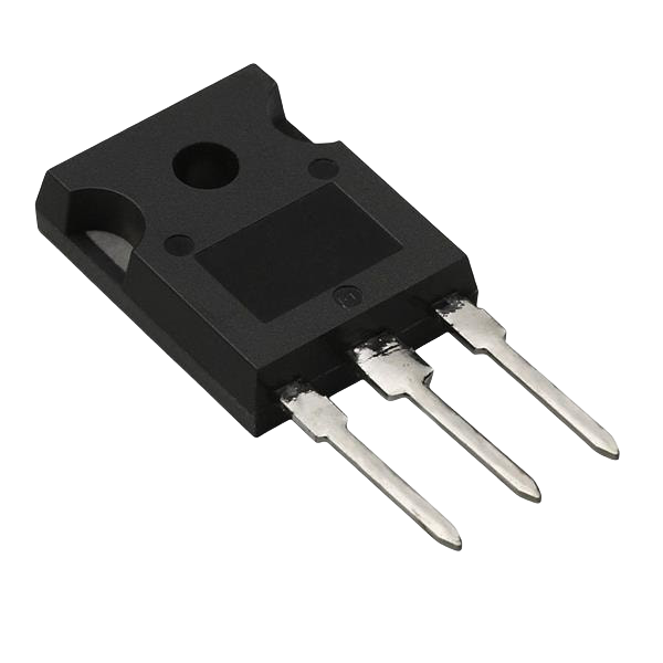
Thermal Management: Advanced packaging technologies (e.g., TO-220, SOP-8L) ensure efficient heat dissipation, reducing thermal runaway risks in compact charger designs.
By leveraging these features, YFW enables charger manufacturers to achieve higher power densities, faster charging speeds, and enhanced reliability.
As EV charging evolves toward 800V architectures and ultra-fast charging (UFC), NMOS technology must adapt to new demands:
Wide Bandgap Integration: While silicon carbide (SiC) MOSFETs are gaining traction in high-power applications, silicon-based NMOS remains cost-effective for mid-range chargers. YFW is exploring hybrid solutions that combine Si NMOS with SiC diodes to optimize performance and cost.
Intelligent Control: Future NMOS devices will integrate with AI-driven algorithms to dynamically adjust switching parameters, improving efficiency across varying load conditions.
Standardization: With global charging standards like CCS and CHAdeMO converging, YFW’s NMOS products are designed to meet interoperability requirements, ensuring seamless integration into multi-brand charging networks.
NMOS transistors are indispensable in modern EV charging systems, driving efficiency, safety, and scalability. YFW Microelectronics’ commitment to innovation—through high-performance NMOS solutions and robust thermal management—positions the company as a key enabler of the global EV transition. As charging infrastructure continues to expand, YFW remains dedicated to delivering reliable, cutting-edge semiconductor technologies that power the future of mobility.
For more information on YFW’s NMOS products for EV charging, visit www.yfwdiode.com