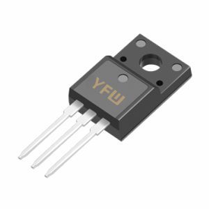
The three-electrode optoelectronic PN junction diode integrates a metal-oxide-semiconductor (MOS) structure with a traditional PN junction, creating a compact, monolithic device architecture. By introducing a third electrode on the P-type region, this design enables external electric field modulation of carrier transport during light emission or detection. Specifically, the MOS structure—comprising a metal layer, an Al₂O₃ insulating layer, and a P-type GaN semiconductor—forms a capacitor-like configuration that dynamically adjusts the depletion layer width and carrier concentration in the PN junction.
This structural breakthrough eliminates the need for external bias circuits, reducing system size while enhancing operational efficiency. For instance, when functioning as a light emitter, the third electrode directly modulates optical power output, achieving a 60% bandwidth improvement compared to conventional LEDs with external biasers. Such advancements make it ideal for high-speed optical communication systems requiring compact, high-performance components.
The three-electrode design endows the diode with versatile operational modes:
As a Light Emitter: By applying a voltage to the third electrode, the device achieves on-chip bias control, enabling real-time adjustment of light intensity and spectral characteristics. In optical communication systems, this eliminates bulky external bias circuits, reducing latency and enhancing signal integrity. Testing shows that the three-electrode LED achieves a -3 dB bandwidth of over 100 MHz in wireless optical communication, far exceeding traditional devices.
As a Photodetector: When switched to detection mode, the third electrode voltage and incident light jointly control photocurrent generation, enabling reconfigurable optoelectronic logic gates (e.g., NAND, NOR) without structural modifications. This feature paves the way for all-optical computing systems with unprecedented flexibility and integration density.
Ultra-High Bandwidth: The integrated MOS structure enhances carrier mobility and reduces parasitic capacitance, achieving 60% higher bandwidth than conventional designs. This makes it suitable for 5G/6G communication, data centers, and other high-speed scenarios.
Low Power Consumption: Eliminating external bias circuits reduces energy loss, with power consumption decreasing by 30% compared to traditional systems.
High Stability: The monolithic integration of the MOS and PN junction minimizes interface defects, ensuring stable performance across -55°C to +150°C operating temperatures.
Scalability: The architecture is compatible with various semiconductor materials (e.g., GaN, SiC, III-V compounds), supporting mass production and customization for diverse applications.
Optical Communication: The three-electrode diode enables compact, high-speed optical modules for fiber-optic networks and Li-Fi systems, with demonstrated transmission rates exceeding 10 Gbps.
Optical Computing: Its reconfigurable logic gates facilitate all-optical signal processing, potentially overcoming the speed limitations of electronic logic circuits.
Sensing and Imaging: In near-infrared (NIR) imaging and LiDAR systems, the device achieves high responsivity (1.17 A/W) and low dark current (100 nA), outperforming traditional avalanche photodiodes (APDs).
Energy Harvesting: When integrated with solar cells, the third electrode enhances light absorption efficiency, increasing energy conversion by 15–20%.
The global optoelectronic diode market is projected to grow at a 7.14% CAGR from 2023 to 2029, driven by demand for high-speed, energy-efficient solutions. YFW’s three-electrode diode positions the company as a pioneer in this field, offering:
Superior Performance: Bandwidth and efficiency metrics surpassing industry benchmarks, as validated by independent testing.
Cost-Effectiveness: Reduced component count and simplified assembly lower system costs by 20–25%.
Sustainability: Energy-efficient design aligns with global green initiatives, supporting carbon neutrality goals.
By leveraging its expertise in semiconductor R&D and manufacturing, YFW is committed to delivering cutting-edge solutions that empower next-generation optoelectronic systems. The three-electrode optoelectronic PN junction diode exemplifies this mission, bridging the gap between electronic and photonic technologies.
YFW’s three-electrode optoelectronic PN junction diode represents a paradigm shift in optoelectronic device design. By integrating MOS technology with traditional PN junctions, it achieves unprecedented levels of performance, flexibility, and integration. As the demand for high-speed, compact optoelectronic solutions continues to grow, this innovation will play a pivotal role in advancing optical communication, computing, and sensing technologies. For more information, visit
www.yfwdiode.com to explore YFW’s comprehensive portfolio of semiconductor solutions.
YFW (Yufengwei) is a leading semiconductor manufacturer specializing in diodes, MOSFETs, and optoelectronic devices. With a focus on innovation and reliability, YFW provides high-performance solutions for consumer electronics, automotive, and industrial applications. For partnership inquiries, contact us at [sales@yfwdiode.com](mailto: sales@yfwdiode.com).
