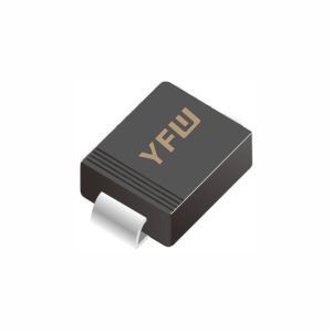
Photodiodes operate based on the photovoltaic effect within a PN junction. When photons strike the junction, they generate electron-hole pairs, which are rapidly separated by the built-in electric field. This process occurs within the depletion layer, a region optimized for minimal carrier recombination. YFW’s photodiodes feature a thin, wide depletion layer (as seen in PIN diode designs), which maximizes the absorption of incident light while minimizing carrier diffusion time.
In contrast, photoresistors rely on the photoconductive effect. These devices, typically made of materials like cadmium sulfide (CdS), increase conductivity when exposed to light by exciting electrons from the valence band to the conduction band. However, this process involves carrier generation and recombination, which inherently introduces delays. The absence of a built-in electric field in photoresistors means carriers must migrate through the material via diffusion, a slower mechanism.
The time response of a photodiode is governed by two key factors:
RC Time Constant: Determined by the junction capacitance (C) and load resistance (R). YFW’s photodiodes are designed with ultra-low junction capacitance (e.g., through planar 工艺), ensuring a small RC time constant.
Carrier Transit Time: The time required for carriers to traverse the depletion layer. YFW’s optimized depletion layer thickness and high electric field (via reverse biasing) accelerate this process, achieving sub-microsecond to nanosecond-level responses.
Photoresistors, on the other hand, suffer from millisecond-to-second response times due to:
Recombination Delays: Once light is removed, carriers in photoresistors recombine slowly, prolonging the recovery time.
RC Limitations: The high resistance of photoresistors (often in the MΩ range) combined with parasitic capacitance leads to large RC time constants.
YFW’s photodiodes incorporate cutting-edge materials and designs to enhance speed:
Silicon and III-V Semiconductors: These materials offer superior carrier mobility and absorption coefficients, enabling faster charge separation.
Reverse Biasing: By applying a reverse voltage, YFW photodiodes widen the depletion layer and reduce junction capacitance, further optimizing response speed.
Surface Passivation: This technique minimizes surface defects and dark current, ensuring stable, high-speed performance even in low-light conditions.
Photoresistors, typically made of polycrystalline materials like CdS, lack such precision. Their grain boundaries and structural imperfections introduce trapping sites, which slow down carrier transport.
YFW’s fast-response photodiodes excel in scenarios demanding real-time precision:
Optical Communications: In fiber-optic networks, YFW photodiodes enable gigabit-per-second data transfer by accurately capturing high-frequency light pulses.
Industrial Sensing: For robotics and automation, their nanosecond-level rise times ensure seamless object detection and motion tracking.
Medical Devices: In pulse oximeters and diagnostic tools, YFW photodiodes deliver rapid, reliable measurements of physiological signals.
Photoresistors, while cost-effective, are ill-suited for these applications. Their slow response limits them to basic tasks like ambient light sensing in streetlights or camera exposure control.
The faster time response of photodiodes over photoresistors stems from fundamental differences in their operational principles, material properties, and structural design. YFW’s photodiodes leverage advanced semiconductor engineering—including optimized depletion layers, low capacitance, and high-purity materials—to achieve industry-leading response speeds. For applications requiring precision, reliability, and speed, YFW’s photodiodes are the definitive choice.
