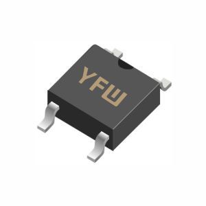
At their core, photodiodes rely on the photovoltaic effect within a PN junction. When photons with sufficient energy strike the junction, they excite electrons from the valence band to the conduction band, creating electron-hole pairs. In reverse-biased conditions, these carriers are swept across the depletion region by the internal electric field, generating a photocurrent proportional to the incident light intensity. The efficiency of this process is governed by responsivity (A/W) and quantum efficiency (%), which quantify the conversion of light power to electrical current .
Key parameters include:
Dark Current: The residual current in the absence of light, minimized through advanced material engineering.
Response Time: Determined by carrier drift and diffusion, critical for high-speed applications like fiber optics.
Featuring an intrinsic (I) layer sandwiched between P and N regions, PIN photodiodes offer broad spectral sensitivity and high-speed response. The thick I-layer increases the depletion width, reducing capacitance and enhancing charge collection efficiency. These devices are ideal for applications requiring linearity and low noise, such as optical receivers and medical imaging .
APDs leverage avalanche multiplication under high reverse bias to amplify photocurrent internally. This makes them highly sensitive to weak light signals, with gains up to 1000×. However, their design demands precise control over breakdown voltage to avoid excessive noise . APDs are widely used in long-haul fiber-optic networks and lidar systems.
With a metal-semiconductor junction, Schottky photodiodes exhibit ultra-fast response times (sub-nanosecond) and low forward voltage drops (0.3–0.6V). Their metal contact enhances absorption of shorter wavelengths, making them suitable for UV detection and high-frequency applications like microwave photonics .
The choice of semiconductor material dictates a photodiode’s spectral range, efficiency, and durability.
Dominates consumer electronics due to its low cost and high quantum efficiency in the visible spectrum (400–1100 nm). However, Si’s bandgap limits its sensitivity to infrared light.
Ge extends detection to near-infrared (NIR) wavelengths (800–1700 nm), making it suitable for optical communication. However, its higher dark current and lower speed compared to III-V materials restrict high-performance applications.
Gallium Arsenide (GaAs): Offers broad spectral coverage (400–1800 nm) and high electron mobility, ideal for high-speed and high-power applications.
Indium Phosphide (InP): Optimized for long-wavelength NIR (1000–1700 nm), critical for dense wavelength-division multiplexing (DWDM) systems.
InGaAs: A ternary alloy combining GaAs and InP, InGaAs provides high responsivity and low noise across 900–2600 nm, making it the gold standard for fiber-optic receivers .
YFW’s focus on third-generation semiconductors like Silicon Carbide (SiC) and Gallium Nitride (GaN) enables photodiodes with superior temperature stability and power handling. These materials are reshaping applications in harsh environments, such as automotive LiDAR and industrial sensing .
Photodiodes are indispensable in modern optoelectronics, with advancements in materials and designs continuously pushing performance boundaries. YFW’s expertise in semiconductor engineering ensures reliable, high-quality photodiodes tailored to diverse industries. By combining precision manufacturing with innovative materials like InGaAs and SiC, YFW delivers solutions that excel in speed, sensitivity, and durability—driving the future of optical technology.
For cutting-edge photodiode products and custom solutions, visit YFW Diodes 