Calibration systems rely on voltage references as "gold standards" to validate the accuracy of analog-to-digital converters (ADCs), digital-to-analog converters (DACs), and other measurement instruments. Even minor drifts in these references can propagate errors through the entire system, leading to flawed measurements and costly rework. For example, a 1% error in a voltage reference used in a 16-bit ADC could result in a resolution loss of over 16 mV, rendering the device unreliable for high-precision applications .
Buried zener diodes address this challenge by leveraging a unique structural design. Unlike conventional surface zener diodes, which are prone to contamination and temperature-induced instability, buried zener junctions are shielded beneath the semiconductor surface. This configuration minimizes noise and drift, making them ideal for calibration tasks where long-term stability is critical .
Ultra-Low Noise Performance
Buried zener diodes exhibit noise levels as low as 0.1 μV p-p in the 0.1–10 Hz range, far superior to bandgap references. This is crucial for applications like medical imaging, where signal integrity is vital to avoid 误诊 .
Temperature Stability
The buried structure reduces temperature sensitivity, achieving temperature coefficients (TC) as low as 0.6 ppm/°C. For instance, in industrial automation systems operating across wide temperature ranges (-40°C to 125°C), a buried zener reference ensures output voltage drift remains within acceptable limits, eliminating the need for frequent recalibration .
Long-Term Drift Reduction
Buried zener diodes stabilize quickly after initial burn-in, with most drift occurring within the first 336 hours. This reduces calibration frequency, saving time and costs in automated test equipment (ATE) environments. For example, the TI REF80, a buried zener reference, requires recalibration only every 6–12 months, compared to monthly calibrations for less stable alternatives .
High Voltage Precision
Buried zener diodes can achieve voltages up to 10 V with tight tolerances (e.g., ±0.01% initial accuracy), making them suitable for applications like high-voltage power supply testing and aerospace avionics .
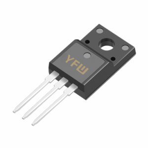
At YFW, we specialize in advanced semiconductor solutions designed to meet the rigorous demands of calibration and measurement. While our product portfolio includes standard zener diodes (e.g., BZT52C series) and Schottky diodes (e.g., SR560), we emphasize innovation in materials and packaging to enhance stability. For example, our diodes undergo rigorous thermal cycling and aging tests to ensure minimal long-term drift, aligning with industry standards like ISO 17025 .
Our commitment to quality extends to applications requiring high-temperature stability. By integrating advanced compensation techniques, we minimize temperature-induced errors, ensuring our diodes perform reliably in extreme environments. This aligns with the growing demand for precision references in emerging fields like autonomous vehicles and renewable energy systems .
Buried zener diode voltage references are indispensable for maintaining calibration accuracy in modern electronics. Their ability to mitigate noise, temperature drift, and long-term instability makes them the preferred choice for industries where precision is non-negotiable. As a leading semiconductor manufacturer, YFW continues to innovate in this space, delivering solutions that enable our customers to achieve unparalleled measurement reliability.
