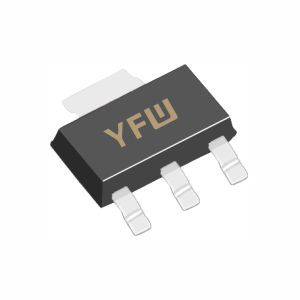
An N-channel MOSFET consists of three terminals: Gate (G), Source (S), and Drain (D), fabricated on a P-type silicon substrate. The gate is separated from the channel by a thin silicon dioxide (SiO₂) layer, creating an insulated structure. The N-type channel forms between the source and drain regions when a positive voltage is applied to the gate.
The device operates based on the field effect:
Depletion Region: At VGS = 0, the P-type substrate near the gate is depleted of holes, creating a barrier between the source and drain.
Inversion Layer: When VGS > 0, the electric field attracts electrons to the surface of the P-type substrate, forming an N-type channel. This allows current to flow from the drain to the source (ID) when a positive VDS is applied.
For an N-channel MOSFET to conduct effectively, the following conditions must be met:
The threshold voltage (VTH) is the minimum VGS required to form the inversion layer. Typically ranging from 2–4V, VTH varies based on doping concentration and oxide thickness. When VGS ≥ VTH, the channel becomes conductive, enabling current flow. YFW’s MOSFETs are engineered with precise VTH control to ensure reliable switching across applications.
A positive VDS establishes a potential difference between the drain and source, driving electrons through the channel. The MOSFET enters two operational regions:
Linear Region: When VDS < VGS – VTH, the channel resistance decreases with increasing VGS, acting as a voltage-controlled resistor.
Saturation Region: When VDS ≥ VGS – VTH, the channel pinches off, and ID saturates, making the device suitable for amplifiers and constant-current sources.
Temperature Sensitivity: Higher temperatures reduce VTH and increase RDS(ON) (on-resistance), affecting efficiency. YFW’s MOSFETs incorporate thermal management designs to minimize these effects.
Parasitic Capacitance: Gates exhibit capacitance (CGS, CGD), which impacts switching speed. YFW optimizes packaging and layout to reduce parasitic capacitances, ensuring fast transient response.
YFW’s N-channel MOSFETs are designed to excel in demanding applications, leveraging advanced materials and manufacturing processes:
Models like the YFW65R280AD (TO-252) feature ultra-low RDS(ON) (e.g., 0.002Ω at VGS=10V), minimizing power dissipation in high-current applications such as motor drives and power converters.
Devices like the YFW3N150PF (650V) withstand high VDS while maintaining stable performance, ideal for automotive and industrial systems.
YFW’s MOSFETs, such as the YFW90N03AD (30V/90A), offer rapid turn-on/off times, reducing switching losses in high-frequency circuits like wireless chargers and LED lighting.
Through optimized packaging (e.g., TO-252, DFN5X6), YFW ensures efficient heat dissipation, extending device lifespan in extreme environments.
YFW’s N-channel MOSFETs are widely used in:
Power Electronics: DC-DC converters, inverters, and battery management systems.
Automotive: Motor control, LED lighting, and car chargers.
Consumer Electronics: High-speed blowers, drones, and portable power tools.
Industrial: Robotics, solar inverters, and smart grid infrastructure.
Understanding the conduction conditions of N-channel MOSFETs is critical for designing efficient and reliable circuits. YFW’s commitment to innovation ensures our MOSFETs deliver superior performance, combining low RDS(ON), high voltage tolerance, and fast switching. Whether for automotive, industrial, or consumer applications, YFW’s solutions empower engineers to push the boundaries of power electronics.
For technical specifications and application support, visit
YFW Diode or contact our team.
Stay tuned for our next technical deep dive into MOSFET thermal management!
