JFET Pin Identification Guide for Circuit Designers
Date:2025-04-22 Categories:Product knowledge Hits:1055 From:Guangdong Youfeng Microelectronics Co., Ltd
Most JFETs follow specific pin configurations based on their package:
TO-92 (Plastic Package): Hold the device with the flat side facing you. The pins typically align as Drain (D), Gate (G), Source (S) from left to right . However, variations exist (e.g., some manufacturers use G-D-S).
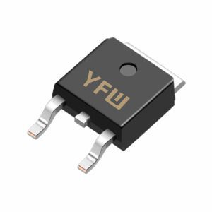
TO-220 (Metal Package): The tab is connected to the Drain (D), with Gate (G) and Source (S) adjacent .
Four-Pin JFETs: An extra pin serves as a shielding electrode (grounded during operation) .
Use a digital multimeter (DMM) in
Diode Test Mode or
R×1kΩ resistance mode:
JFETs are symmetrical in most cases, meaning S and D can be interchanged without affecting functionality . Verify this by measuring the resistance between S and D—it should be low and consistent in both directions .
For critical applications, assess the JFET’s transconductance (gm) using the R×100Ω mode:
Safety: Always power off the circuit before testing.
ESD Protection: While JFETs are less sensitive than MOSFETs, avoid static discharge during handling.
Documentation: Refer to the datasheet for exact pinouts, as variations exist across manufacturers.
As a trusted semiconductor provider,
YFW Microelectronics ensures precision-engineered JFETs with consistent pin configurations for reliable performance. For tailored solutions, explore our
product lineup or contact our technical support.
Previous:
Classification, Structure, and Principle of MOSFET
Next:
Understanding Enhancement vs. Depletion Mode FETs for Advanced Circuit Design

