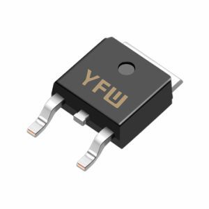
Field - effect transistors (FETs) are essential components in modern electronic circuits, and YFW FETs are well - recognized for their high - quality performance. However, to ensure their reliable and efficient operation, several important precautions should be taken into account.
YFW FETs are highly sensitive to electrostatic discharge. When storing these components, they should be placed in anti - static containers or bags. During handling, operators should wear anti - static wrist straps or use anti - static mats to prevent the build - up and discharge of static electricity. Even a small electrostatic shock can damage the delicate semiconductor structure of the FET, leading to malfunction or reduced lifespan.
The storage environment should have controlled temperature and humidity levels. High temperatures can cause thermal stress to the FETs, affecting their electrical properties. Excessive humidity may lead to corrosion of the pins and internal components. It is recommended to store YFW FETs in a dry and cool place, with a temperature range of around 20 - 30°C and a relative humidity of less than 60%.
Proper biasing is crucial for the normal operation of YFW FETs. Incorrect biasing can result in the FET operating outside its intended region, such as the cutoff or saturation region, leading to distortion of the output signal. For example, in a common - source amplifier circuit, the gate - source voltage (\(V_{GS}\)) must be carefully set to ensure that the FET operates in the linear region. This usually involves using appropriate resistors in a voltage - divider or self - biasing configuration.
The input and output impedance of the circuit connected to the YFW FET should be properly matched. A mismatch in impedance can cause signal reflection and loss, reducing the efficiency of the circuit. For instance, if the input impedance of the circuit is too low compared to the FET's input impedance, it can load the input signal and distort it. Similarly, an improper output load can affect the output voltage and power of the FET.
YFW FETs have a maximum power dissipation rating. Exceeding this rating can cause the device to overheat and potentially fail. When designing the circuit, the power dissipated by the FET under normal operating conditions should be calculated. This includes the power dissipated in the drain - source channel (\(P = V_{DS}I_D\)) and any additional power due to biasing resistors. Adequate heat - sinking measures, such as using heat sinks or fans, should be taken if the power dissipation is close to or exceeds the rated value.
When soldering YFW FETs onto the printed circuit board (PCB), the soldering temperature and time should be strictly controlled. High - temperature soldering for an extended period can damage the FET. The recommended soldering temperature for most YFW FETs is around 260 - 300°C, and the soldering time should be kept within 3 - 5 seconds per pin.
During the installation process, avoid applying excessive mechanical stress to the FET. Bending or twisting the pins can cause internal damage to the device. When inserting the FET into the PCB sockets or soldering it, handle it gently to prevent any physical deformation.
Before using YFW FETs in a circuit, it is advisable to perform basic electrical tests. This can include measuring the drain - source resistance, gate - source capacitance, and other relevant parameters to ensure that the device is functioning properly.
During the operation of the circuit, monitor the key electrical parameters of the YFW FET, such as the drain current (\(I_D\)), drain - source voltage (\(V_{DS}\)), and gate - source voltage (\(V_{GS}\)). Any abnormal changes in these parameters may indicate a problem with the FET or the circuit.
By following these precautions, users can ensure the reliable and long - term operation of YFW field - effect transistors in various electronic applications.
