Date:2025-04-09 Categories:Product knowledge Hits:660 From:Guangdong Youfeng Microelectronics Co., Ltd
Field Effect Transistor (FET) is a voltage controlled device that has an input voltage to control the variation of output current. It has the advantages of high input impedance, low noise, large dynamic range, and low temperature coefficient, and is therefore widely used in various electronic circuits.
1、 The structural principle and characteristics of field-effect transistors
Field effect transistors have two types of structures: junction type and insulated gate, each of which has two types of conductive channels: N-channel and P-channel.
1. Junction Field Effect Transistor (JFET)
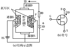
(1) The structural principle and symbols are shown in Figure 1. Two electrodes, drain electrode D and source electrode S, are led out at both ends of the N-type silicon rod, and a P region is made on each side of the silicon rod to form two PN junctions. In the P region, electrodes are led out and connected together, called gate Go, which forms an N-channel field-effect transistor
1、 The structural principle and characteristics of field-effect transistors
Field effect transistors have two types of structures: junction type and insulated gate, each of which has two types of conductive channels: N-channel and P-channel.
1. Junction Field Effect Transistor (JFET)
(1) The structural principle and symbols are shown in Figure 1. Two electrodes, drain electrode D and source electrode S, are led out at both ends of the N-type silicon rod, and a P region is made on each side of the silicon rod to form two PN junctions. In the P region, electrodes are led out and connected together, called gate Go, which forms an N-channel field-effect transistor
(2) Characteristic curve
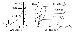
1) Transfer characteristics
Figure 2 (a) shows the gate voltage drain current characteristic curve of an N-channel junction field-effect transistor, known as the transfer characteristic curve, which is very similar to the dynamic characteristic curve of an electron diode. It shows the drain source current when the gate voltage VGS=0. Represented by IDSS. When VGS becomes negative, ID gradually decreases. The gate voltage with an ID close to zero is called the pinch off voltage, represented by VP. In the range of 0 ≥ VGS ≥ VP, the relationship between ID and VGS can be approximately expressed as:
ID=IDSS(1-|VGS/VP|)
Its transconductance gm is: gm=(△ ID/△ VGS) | VDS=constant micro (micro ohm)|
In the formula: △ ID - incremental drain current (microamperes)
------△ VGS - incremental gate source voltage (volts)
2) Drain characteristics (output characteristics)
Figure 2 (b) shows the drain characteristic curve of the field-effect transistor, which is very similar to the output characteristic curve of the transistor.
① The variable resistance region (region I in the figure) has a relatively small VDS in region I, and the communication resistance changes with the gate voltage VGS, hence it is called the variable resistance region. When the gate voltage is constant, the communication resistance is constant, and ID increases approximately linearly with VDS. When VGS<VP, the resistance between the drain and source is large (turned off). IP=0; When VGS=0, the resistance between the drain and source is very small (conductive), ID=IDSS。 This characteristic gives the field-effect transistor a switching function.
② When the drain voltage VDS continues to increase to VDS>| VP | in the constant current region (region II), the drain current and IP remain basically unchanged after reaching saturation. This region is called the constant current region or saturation region. Here, the drain characteristic curves of different VGS are approximately parallel lines, that is, ID and VGS have a linear relationship, so it is also called the linear amplification region.
③ If VDS continues to increase in the breakdown region (region III in the figure), exceeding the voltage that the PN junction can withstand and being broken down, the drain current ID will suddenly increase. If no limiting measures are taken, the diode will burn out.
2. Insulated gate field-effect transistor
It is composed of metal, oxide, and semiconductor, so it is also known as metal oxide semiconductor field-effect transistor, abbreviated as MOS field-effect transistor.
(1) Structural principle
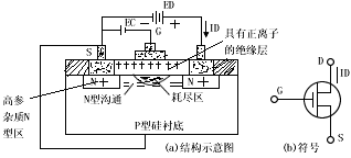
Its structure, electrodes, and symbols are shown in Figure 3. A P-type thin silicon wafer is used as the substrate, and two high impurity N-type regions are diffused on it as the source S and drain D. Cover the surface of the silicon wafer with a layer of insulation, and then use aluminum metal to lead out an electrode G (gate). As the gate is insulated from other electrodes, it is called an insulated gate field-effect transistor.
When manufacturing pipes, a large number of positive ions are generated in the insulation layer through the process, so that more negative charges can be induced on the other side of the interface. These negative charges connect the high permeability impurity N region, forming a conductive channel, and even at VGS=0, there is a large drain current ID. When the gate voltage changes, the amount of induced charge in the channel also changes, and the width of the conductive channel also changes accordingly. Therefore, the drain current ID changes with the change of gate voltage.
There are two ways to operate field-effect transistors: the dissipative type has a large drain current when the gate voltage is zero, and the enhanced type has a drain current when the gate voltage is zero and the drain current is also zero.
(2) Characteristic curve
1) Transfer characteristics (gate voltage leakage current characteristics)
Figure 4 (a) shows the transfer behavior curve of an N-channel depletion type insulated gate field-effect transistor, where Vp is the pinch off voltage (gate source cut-off voltage); IDSS stands for saturated leakage current.
Figure 4 (b) shows the transfer characteristic curve of an N-channel enhanced insulated gate field-effect transistor, where Vr is the turn-on voltage. When the gate voltage exceeds VT, the drain current begins to significantly increase.
2) Drain characteristics (output characteristics)
Figure 5 (a) shows the output characteristic curve of an N-channel depletion type insulated gate field-effect transistor.
Figure 5 (b) shows the output characteristic curve of an N-channel enhanced insulated gate field-effect transistor.
In addition, there are field-effect transistors with N substrate P channel (see Figure 1), which are also divided into two types: depletion type and enhancement type,
Classification of various field-effect devices, voltage symbols, and main volt ampere characteristics (transfer characteristics, output characteristics)
2、 Main parameters of field-effect transistor
1. Pinch off voltage VP
When VDS is a fixed value that makes IDS equal to a small current, the bias voltage VGS applied to the gate is the pinch off voltage VP.
2. Saturated leakage current IDSS
Under the condition of short circuit between the source and gate, the drain current when the voltage applied between the drain and source is greater than VP is called IDSS.
3. Breakdown voltage BVDS
The maximum voltage that can be sustained between the drain and source, i.e. the VDS corresponding to the saturation current of the drain starting to rise and entering the breakdown region.
4. DC input resistor RGS
At a certain gate source voltage, the DC resistance between the gate and source is represented by the current flowing through the gate. The RGS of junction field-effect transistors can reach 1000000000 ohms, while the RGS of insulated gate field-effect transistors can exceed 1000000000000 ohms.
5. Low frequency transconductance gm
The ratio of the micro variable of drain current to the micro variable of gate source voltage that causes this change is called transconductance, that is
gm= △ID/△VGS
Previous: Classification, Structure, and Principle of MOSFET
Next: Main characteristic parameters of field-effect transistors