Date:2025-03-20 Categories:Product knowledge Hits:557 From:Guangdong Youfeng Microelectronics Co., Ltd
Advantages of Schottky diodes in circuit applications
Schottky diode is a semiconductor component made of metal material as the positive stage and N-type semiconductor as the negative stage, using the potential barrier generated on the surface of both to have the characteristics of a rectifier. It is a hot carrier diode. Schottky diode is mainly used as a rectifier diode, freewheeling diode, maintenance diode, etc. in power circuits, and is mainly used in low-voltage and high current power circuits, such as power transformers, soft starters, inverter power supplies, and fiber optic communication. Widely used in small signal circuits of semiconductor radios, recorders, televisions, and communication devices, today let's take a look at the application advantages of Schottky diodes in circuits:
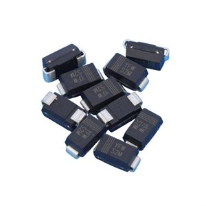
Schottky diode
Schottky diode is a metal material semiconductor component made by using precious metals such as gold, silver, aluminum, platinum as the positive stage and N-type semiconductor B as the negative stage, and utilizing the potential barrier generated on the surfaces of the two to possess the characteristics of a rectifier. Due to the presence of many electronic devices in N-type semiconductors, precious metals only have a small amount of free charge, so electronic devices diffuse from high concentration B to low concentration A.
There is no cavitation in metal material A, so there will be no diffusion of cavitation from A to B for fitness exercise. As electronic devices continue to diffuse from B to A, the concentration of surface electronic devices in B gradually decreases, and the balance of surface charges is disrupted, thus creating a potential barrier with an electric field direction of B → A. However, in this electrostatic field effect, the electronic components in A can also cause drift fitness movements from A to B, thereby weakening the electrostatic field generated by external diffusion fitness movements. When a space charge region with a certain overall width is created, the static electric field causes electronic device drift and fitness movement, and the concentration value difference causes electronic device external diffusion and fitness movement to achieve relative balance, resulting in Schottky barrier.
The internal power circuit structure of a typical Schottky rectifier diode is based on an N-type semiconductor substrate, on which an N-epitaxial layer doped with arsenic is formed. Anodizing uses raw materials such as molybdenum or aluminum to create a barrier layer. Use silicon dioxide (SiO2) to remove the static electric field in the edge area and improve the compressive strength of the water pipe.
The N-type substrate has a relatively small on state resistor, and its inclusion concentration is 100% higher than that of the H-layer. Generate an N+negative electrode layer underneath the substrate, which reduces the circuit resistance of the negative electrode. According to the main parameters of the optimized structure, a specific energy barrier is generated between the N-type substrate and the anodized metal material, as shown in the following figure. When a forward bias is applied on both sides of the Schottky barrier (anode oxidized metal material plug positive stage, N-type substrate plug negative stage), the Schottky barrier layer becomes smaller and its internal resistance decreases; On the contrary, if a reverse bias is applied on both sides of the Schottky barrier, the Schottky barrier layer becomes larger and its internal resistance increases.
Previous: Classification, Structure, and Principle of MOSFET
Next: What is the principle and construction working principle of Schottky diode