Date:2025-02-18 Categories:Product knowledge Hits:422 From:Guangdong Youfeng Microelectronics Co., Ltd
A bipolar junction transistor is equivalent to two back-to-back diode PN junctions. The forward biased EB junction injects holes from the emitter into the base region, most of which can reach the boundary of the collector junction and reach the collector region under the action of the reverse biased CB junction potential barrier electric field, forming a collector current IC. In a common emitter transistor circuit, the emitter junction is forward biased in the base circuit, resulting in a small voltage drop. The majority of the applied bias voltage between the collector and emitter is applied to the reverse biased collector junction. Due to the small VBE, the base current is approximately IB=5V/50 k Ω=0.1mA.
If the common emitter current amplification factor of the transistor β=IC/IB=100, and the collector current IC=β * IB=10mA. There is a voltage drop VRC=10mA * 500 Ω=5V across a 500 Ω collector load resistor, while the voltage drop between the collector and emitter of a transistor is VCE=5V. If an alternating small current ib is added to the base bias circuit, a corresponding alternating current ic will appear in the collector circuit, with c/ib=β, achieving the current amplification effect of a bipolar transistor.
The basic working principle of metal oxide semiconductor field-effect transistor relies on the electric field effect on the surface of the semiconductor to induce conductive channels in the semiconductor for operation. When the gate G voltage VG increases, The majority carriers on the surface of p-type semiconductors, including holes, gradually decrease and deplete, while electrons gradually accumulate to the inversion. When the surface reaches inversion, the electron accumulation layer will form a conductive channel between the n+source region S and the n+drain region D. When VDS ≠ 0, there is a large current IDS flowing between the source and drain electrodes. The gate source voltage required to achieve strong inversion on the semiconductor surface is called the threshold voltage VT. When VGS>VT and different values are taken, the conductivity of the inversion layer will change, and different IDS will be generated under the same VDS, achieving the control of gate source voltage VGS on source drain current IDS.
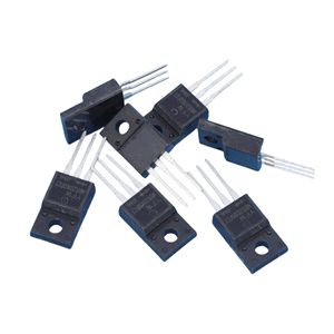
Test the transistor with a multimeter
(1) Distinguish the type of base and diode
Select the R * 100 (or R * 1K) ohm range. First, connect the red probe to one pin and the black probe to the other pin to measure two resistance values. Then, connect the red probe to the other pin and repeat the above steps to measure another set of resistance values. Repeat this process three times, and there is a set of two resistance values that are both very small. The red probe corresponding to this set of values is connected to the base, and the transistor is PNP type; On the contrary, if a black probe is connected to a pin and the above method is repeated, if both resistance values are measured to be small, the corresponding black probe is the base and the diode is NPN type.
(2) Discriminate collector electrode
Because when the emitter and collector of a transistor are correctly connected, β is larger (the pointer swings more), and when they are reversed, β is much smaller. Therefore, let's assume a collector connected in ohms range (for NPN transistors, connect the emitter to the black probe and the collector to the red probe). When measuring, hold the base and the assumed collector with your hand. The two poles should not be in contact. If the pointer swings greatly and the pointer swings less after swapping the two poles, it indicates that the assumption is correct, and the collector and emitter are determined accordingly.
(2) Estimation of current amplification factor β
Choose the R * 100 (or R * 1K) ohm range and connect the red probe to the emitter and the black probe to the collector for an NPN transistor. When measuring, simply compare the size of the pointer swing between gripping the base and collector with your hand (the two poles cannot touch) and releasing the handle. The larger the swing, the higher the β value.
Previous: Classification, Structure, and Principle of MOSFET