Date:2025-02-17 Categories:Product knowledge Hits:1085 From:Guangdong Youfeng Microelectronics Co., Ltd
Schottky diode is named after its inventor, Dr. Schottky, and is the abbreviation for Schottky Barrier diode (SBD).
What are the special features of Schottky diodes compared to other diodes in terms of their principles and structures?
SBD is not made using the PN junction principle formed by the contact between P-type semiconductor and N-type semiconductor, but using the metal semiconductor junction principle formed by the contact between metal and semiconductor. Therefore, SBD, also known as metal semiconductor (contact) diode or surface barrier diode, is a type of hot carrier diode.
The internal circuit structure of a typical Schottky rectifier diode is based on an N-type semiconductor substrate, on which an N-epitaxial layer doped with arsenic is formed. The anode is made of materials such as molybdenum or aluminum to form a barrier layer. Use silicon dioxide (SiO2) to eliminate the electric field in the edge region and improve the voltage resistance of the diode. N-type substrates have very low on state resistance, and their doping concentration is 100% higher than that of H-layers. An N+cathode layer is formed under the substrate to reduce the contact resistance of the cathode. By adjusting the structural parameters, a Schottky barrier is formed between the N-type substrate and the anode metal, as shown in the figure. When a forward bias is applied across the Schottky barrier (with the anode metal connected to the positive pole of the power supply and the N-type substrate connected to the negative pole of the power supply), the Schottky barrier layer narrows and its internal resistance decreases; On the contrary, if a reverse bias is applied across the Schottky barrier, the Schottky barrier layer widens and its internal resistance increases.
The Schottky rectifier uses only one type of carrier (electron) to transport charges, and there is no accumulation of excess minority carriers outside the barrier. Therefore, there is no charge storage problem (Qrr → 0), which significantly improves the switching characteristics. Its reverse recovery time can be shortened to within 10ns. But its reverse withstand voltage value is relatively low, generally not exceeding 100V when it goes out. Therefore, it is suitable for working under low voltage and high current conditions. By utilizing its low voltage drop characteristic, the efficiency of low voltage and high current rectification (or freewheeling) circuits can be improved.
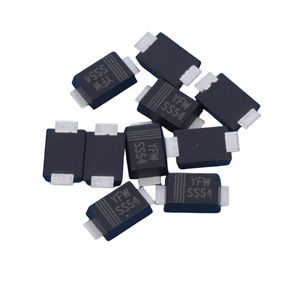
Packaging of Schottky diodes
Schottky diodes are divided into two packaging forms: lead and surface mount (patch). Schottky diodes with lead type packaging are commonly used as high-frequency high current rectifier diodes, freewheeling diodes, or protective diodes. It has two packaging forms: single diode and twin diode. Schottky diodes have three pin extraction methods: common cathode (connecting the negative terminals of two diodes), common anode (connecting the positive terminals of two diodes), and series (connecting the positive terminal of one diode to the negative terminal of the other diode).
Schottky diodes that use surface packaging come in various packaging forms such as single diode, double diode, and triple diode, with A to 19 pin extraction methods.
The main advantages of Schottky diodes include two aspects:
1) Due to the Schottky barrier height being lower than the PN junction barrier height, its forward conduction and forward voltage drop are lower than those of PN junction diodes (about 0.2V lower).
2) Due to SBD being a majority carrier conductive device, there are no issues with minority carrier lifetime and reverse recovery. The reverse recovery time of SBD is only the charging and discharging time of Schottky barrier capacitors, which is completely different from the reverse recovery time of PN junction diodes. Due to the very low reverse recovery charge of SBD, the switching speed is very fast and the switching loss is particularly small, making it particularly suitable for high-frequency applications.
Disadvantages of Schottky diodes
The biggest disadvantage of Schottky diodes is their low reverse bias and high reverse leakage current. For example, Schottky diodes made of silicon and metal materials have a maximum reverse bias rated voltage of only 50V, while the reverse leakage current value has a positive temperature characteristic and is prone to rapidly increase with temperature rise. In practical design, attention should be paid to the hidden concern of thermal runaway. To avoid the above problems, the reverse bias voltage of Schottky diodes in actual use will be much smaller than their rated value. Of course, with the advancement of process technology and Schottky diode technology, the rated value of its reverse bias has also been further increased.
Important parameters of Schottky diodes
Schottky diodes are widely used, especially in switching power supplies. In different applications, different factors need to be considered, and different devices also have differences in performance. Therefore, when selecting Schottky diodes, the following parameters need to be comprehensively considered.
1. Conduction voltage drop VF
VF is the voltage drop across the diode when it conducts in the forward direction. The larger the current passing through the diode, the greater VF; The higher the temperature of the diode, the smaller the VF.
2. Reverse saturated leakage current IR
IR refers to the current flowing through a diode when a reverse voltage is applied across its terminals. Schottky diodes have a larger reverse leakage current, so it is advisable to choose diodes with smaller IR when selecting Schottky diodes.
3. Rated current IF
The average current value calculated based on the allowable temperature rise during long-term operation of a diode.
4. Maximum surge current IFSM
Excessive forward current allowed to flow. It is not a normal current, but an instantaneous current, and this value is quite large.
5. Maximum reverse peak voltage VRM
Even without reverse current, as long as the reverse voltage is continuously increased, the diode will eventually be damaged. This type of reverse voltage that can be applied is not an instantaneous voltage, but a repeatedly applied forward and reverse voltage. The maximum value of the AC voltage applied to the rectifier is a critical factor specified. The maximum reverse peak voltage VRM refers to the maximum reverse voltage that can be applied to avoid breakdown. The current highest VRM value for Schottky is 150V.
6. Maximum DC reverse voltage VR
The maximum reverse peak voltage mentioned above is the peak voltage repeatedly applied, and VR is the value when a DC voltage is continuously applied. For DC circuits, the maximum DC reverse voltage is important for determining the allowable and upper limits.
7. Maximum operating frequency fM
Due to the presence of junction capacitance in PN junctions, their unidirectional conductivity will deteriorate when the operating frequency exceeds a certain value. The fM value of Schottky diodes is relatively high, reaching a maximum of 100GHz.
8. Reverse recovery time Trr
When the working voltage changes from forward voltage to reverse voltage, the ideal situation for diode operation is that the current can be instantly cut off. Actually, it usually requires a slight delay. The amount that determines the current cutoff delay is the reverse recovery time. Although it directly affects the switching speed of the diode, it does not necessarily mean that a small value is enough. That is to say, the time required for the reverse current to decay significantly and approach IR when the diode suddenly reverses direction from conduction. This indicator is crucial when high-power switching transistors operate in high-frequency switching state.
9. Maximum dissipated power P
When current flows through a diode, it absorbs heat, causing its own temperature to rise. In practice, the external heat dissipation also has a significant impact on P. Specifically, it is the product of the voltage applied across the diode, the current flowing through it, and the reverse recovery loss.
Application of Schottky diode in switching power supply
The switching power supply consists of main components such as high-frequency transformer, high-frequency capacitor, high reverse voltage high-power transistor, power rectifier diode, and control IC. The secondary rectifier diode, as an energy consuming component, has high losses (accounting for about 30% of the power consumption) and high heat generation. Its selection is a crucial factor for the overall efficiency and reliability indicators of the power supply. This requires the rectifier diode to have the characteristics of small forward voltage drop VF, small reverse leakage IR, and short recovery time Trr under high-speed and high current working conditions.
For high-frequency rectification of low voltage and high current, Schottky diodes are the best choice (due to their low reverse withstand voltage), and are most commonly used as rectifier output diodes for ± 5V, ± 12V, and ± 15V. The+5V output of computer power supplies mostly uses SR3040, and the+12V output uses SR1660. In addition, the forward voltage drop VF and junction temperature TJ of Schottky diodes exhibit a negative temperature coefficient, so the switching power supplies manufactured with them have high efficiency, low temperature rise, low noise, and high reliability.
Previous: Classification, Structure, and Principle of MOSFET
Next: Application analysis of Schottky diode in power management